- 您現(xiàn)在的位置:買賣IC網(wǎng) > PDF目錄383961 > TMX320DM647ZUT720 (Texas Instruments, Inc.) Digital Media Processor PDF資料下載
參數(shù)資料
| 型號(hào): | TMX320DM647ZUT720 |
| 廠商: | Texas Instruments, Inc. |
| 英文描述: | Digital Media Processor |
| 中文描述: | 數(shù)字媒體處理器 |
| 文件頁(yè)數(shù): | 39/166頁(yè) |
| 文件大小: | 1341K |
| 代理商: | TMX320DM647ZUT720 |
第1頁(yè)第2頁(yè)第3頁(yè)第4頁(yè)第5頁(yè)第6頁(yè)第7頁(yè)第8頁(yè)第9頁(yè)第10頁(yè)第11頁(yè)第12頁(yè)第13頁(yè)第14頁(yè)第15頁(yè)第16頁(yè)第17頁(yè)第18頁(yè)第19頁(yè)第20頁(yè)第21頁(yè)第22頁(yè)第23頁(yè)第24頁(yè)第25頁(yè)第26頁(yè)第27頁(yè)第28頁(yè)第29頁(yè)第30頁(yè)第31頁(yè)第32頁(yè)第33頁(yè)第34頁(yè)第35頁(yè)第36頁(yè)第37頁(yè)第38頁(yè)當(dāng)前第39頁(yè)第40頁(yè)第41頁(yè)第42頁(yè)第43頁(yè)第44頁(yè)第45頁(yè)第46頁(yè)第47頁(yè)第48頁(yè)第49頁(yè)第50頁(yè)第51頁(yè)第52頁(yè)第53頁(yè)第54頁(yè)第55頁(yè)第56頁(yè)第57頁(yè)第58頁(yè)第59頁(yè)第60頁(yè)第61頁(yè)第62頁(yè)第63頁(yè)第64頁(yè)第65頁(yè)第66頁(yè)第67頁(yè)第68頁(yè)第69頁(yè)第70頁(yè)第71頁(yè)第72頁(yè)第73頁(yè)第74頁(yè)第75頁(yè)第76頁(yè)第77頁(yè)第78頁(yè)第79頁(yè)第80頁(yè)第81頁(yè)第82頁(yè)第83頁(yè)第84頁(yè)第85頁(yè)第86頁(yè)第87頁(yè)第88頁(yè)第89頁(yè)第90頁(yè)第91頁(yè)第92頁(yè)第93頁(yè)第94頁(yè)第95頁(yè)第96頁(yè)第97頁(yè)第98頁(yè)第99頁(yè)第100頁(yè)第101頁(yè)第102頁(yè)第103頁(yè)第104頁(yè)第105頁(yè)第106頁(yè)第107頁(yè)第108頁(yè)第109頁(yè)第110頁(yè)第111頁(yè)第112頁(yè)第113頁(yè)第114頁(yè)第115頁(yè)第116頁(yè)第117頁(yè)第118頁(yè)第119頁(yè)第120頁(yè)第121頁(yè)第122頁(yè)第123頁(yè)第124頁(yè)第125頁(yè)第126頁(yè)第127頁(yè)第128頁(yè)第129頁(yè)第130頁(yè)第131頁(yè)第132頁(yè)第133頁(yè)第134頁(yè)第135頁(yè)第136頁(yè)第137頁(yè)第138頁(yè)第139頁(yè)第140頁(yè)第141頁(yè)第142頁(yè)第143頁(yè)第144頁(yè)第145頁(yè)第146頁(yè)第147頁(yè)第148頁(yè)第149頁(yè)第150頁(yè)第151頁(yè)第152頁(yè)第153頁(yè)第154頁(yè)第155頁(yè)第156頁(yè)第157頁(yè)第158頁(yè)第159頁(yè)第160頁(yè)第161頁(yè)第162頁(yè)第163頁(yè)第164頁(yè)第165頁(yè)第166頁(yè)
www.ti.com
P
3.2.2
DSPBOOTADDR Register Description
TMS320DM647/TMS320DM648
Digital Media Processor
SPRS372–MAY 2007
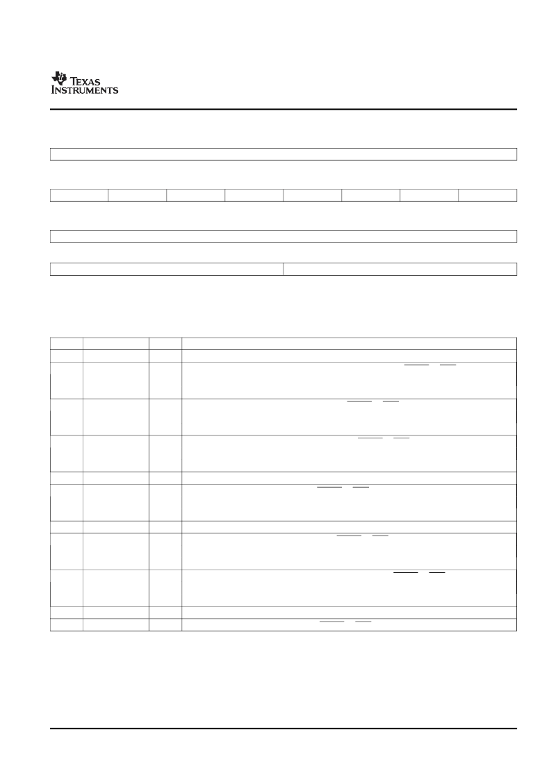
Figure 3-1. BOOTCFG Register
31
24
Reserved
R-0
23
22
21
20
19
18
17
16
AECLKINSEL
PC166
HPIWIDTH
Reserved
FASTBOOT
Reserved
DUHPIEN
EMIFAWIDTH
R-L
R-1
R-L
R-1
R-L
R-L
15
8
Reserved
7
4
3
0
Reserved
BOOTMODE
R-0
R-L
LEGEND: R/W = Read/Write; R = Read only; L = latched; -
n
= value after reset
Table 3-2. BOOTCFG Register Field Descriptions
Bit
31:24
23
Field
Reserved
AECLKINSEL
Value
Description
Reserved
Controls the clock input for EMIFA. Latched from AECLKINSEL at RESET or POR deassertion
EMIFA clocked from internal SYSCLK
EMIFA clocked from outside from AECLKIN
Controls PCI speed. PCI. Latched from PCI66 at RESET or POR deassertion
33 MHz PCI
66 MHz
Controls HPI bus width. Latched from HPIWIDTH at RESET or POR deassertion
16 bit
32 bit
Reserved
Fast Boot. Latched from FASTBOOT at RESET or POR deassertion
No Fast Boot
Fast Boot
Reserved
PCI Enable Default. Latched from UHPIEN at RESET or POR deassertion
UHPI disabled
UHPI enabled
EMIFA CS2 Bus Width Default. Latched from EMIFAWIDTH at RESET or POR deassertion
8-bit
16-bit
Reserved
Boot Mode. Latched from BOOTMOD at RESET or POR deassertion
1
0
22
PCI66
0
1
21
HPIWIDTH
0
1
1
20
19
Reserved
FASTBOOT
0
1
18
17
Reserved
DUHPIEN
0
1
16
EMIFAWIDTH
0
1
15:4
3:0
Reserved
BOOTMODE
The DSPBOOTADDR register contains the upper 22 bits of the C64x+ DSP reset vector. The register
format is shown in
Figure 3-2
and bit field descriptions are shown in
Table 3-3
. DSPBOOTADDR is
readable and writable by software after reset. DSPBOOTADDR Decode: This decode logic determines the
default of the DSPBOOTADDR Register. It can default to either the base address of L2 ROM
(0x00800000) or the base address of EMIFA CS2 (0xA0000000)
Submit Documentation Feedback
Device Configuration
39
相關(guān)PDF資料 |
PDF描述 |
|---|---|
| TMX320DM647ZUT900 | Digital Media Processor |
| TMX320DM648ZUT720 | Digital Media Processor |
| TMX320DM648ZUT900 | Digital Media Processor |
| TMS320LC31PQL | DIGITAL SIGNAL PROCESSORS |
| TMX320C6414TGLZ | FIXED-POINT DIGITAL SIGNAL PROCESSORS |
相關(guān)代理商/技術(shù)參數(shù) |
參數(shù)描述 |
|---|---|
| TMX320DM647ZUT900 | 制造商:TI 制造商全稱:Texas Instruments 功能描述:Digital Media Processor |
| TMX320DM648ACUT7 | 制造商:Texas Instruments 功能描述:- Trays |
| TMX320DM648ACUT9 | 制造商:Texas Instruments 功能描述:- Trays |
| TMX320DM648AZUT7 | 制造商:Texas Instruments 功能描述: |
| TMX320DM648CUT7 | 制造商:Texas Instruments 功能描述:- Trays |
發(fā)布緊急采購(gòu),3分鐘左右您將得到回復(fù)。