- 您現(xiàn)在的位置:買賣IC網(wǎng) > PDF目錄383961 > TMX320DM647ZUT720 (Texas Instruments, Inc.) Digital Media Processor PDF資料下載
參數(shù)資料
| 型號: | TMX320DM647ZUT720 |
| 廠商: | Texas Instruments, Inc. |
| 英文描述: | Digital Media Processor |
| 中文描述: | 數(shù)字媒體處理器 |
| 文件頁數(shù): | 38/166頁 |
| 文件大小: | 1341K |
| 代理商: | TMX320DM647ZUT720 |
第1頁第2頁第3頁第4頁第5頁第6頁第7頁第8頁第9頁第10頁第11頁第12頁第13頁第14頁第15頁第16頁第17頁第18頁第19頁第20頁第21頁第22頁第23頁第24頁第25頁第26頁第27頁第28頁第29頁第30頁第31頁第32頁第33頁第34頁第35頁第36頁第37頁當(dāng)前第38頁第39頁第40頁第41頁第42頁第43頁第44頁第45頁第46頁第47頁第48頁第49頁第50頁第51頁第52頁第53頁第54頁第55頁第56頁第57頁第58頁第59頁第60頁第61頁第62頁第63頁第64頁第65頁第66頁第67頁第68頁第69頁第70頁第71頁第72頁第73頁第74頁第75頁第76頁第77頁第78頁第79頁第80頁第81頁第82頁第83頁第84頁第85頁第86頁第87頁第88頁第89頁第90頁第91頁第92頁第93頁第94頁第95頁第96頁第97頁第98頁第99頁第100頁第101頁第102頁第103頁第104頁第105頁第106頁第107頁第108頁第109頁第110頁第111頁第112頁第113頁第114頁第115頁第116頁第117頁第118頁第119頁第120頁第121頁第122頁第123頁第124頁第125頁第126頁第127頁第128頁第129頁第130頁第131頁第132頁第133頁第134頁第135頁第136頁第137頁第138頁第139頁第140頁第141頁第142頁第143頁第144頁第145頁第146頁第147頁第148頁第149頁第150頁第151頁第152頁第153頁第154頁第155頁第156頁第157頁第158頁第159頁第160頁第161頁第162頁第163頁第164頁第165頁第166頁
www.ti.com
P
3
Device Configuration
3.1 System Module Registers
3.2 Bootmode Registers
3.2.1
Boot Configuration (BOOTCFG) Register
TMS320DM647/TMS320DM648
Digital Media Processor
SPRS372–MAY 2007
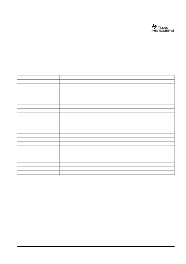
The system module includes status and control registers required for configuration of the device. Brief
descriptions of the various registers are shown in
Table 3-1
. System Module registers required for device
configuration are described in the following sections.
Table 3-1. System Module Register Memory Map
HEX ADDRESS RANGE
0x0204 9000
0x0204 9004
0x0204 9008
0x0204 900C
0x0204 9010
0x0204 9014
0x0204 9018
0x0204 901C
0x0204 9020 -0x0204 9053
0x0204 9054
0x0204 9060 - 0x0204 90A7
0x0204 90A8
0x0204 90AC
0x0204 90B0
0x0204 90B4
0x0204 90B8
0x0204 90BC
0x0204 90C0
0x0204 90C4
0x0204 90C8
0x0204 90CC
0x0204 90D0
0x0204 90D4
REGISTER NAME
PINMUX
DESCRIPTION
Pin multiplexing control 0
Reserved
Boot Address of DSP, decoded by bootloader software for host boots
Boot Complete
Reserved
Device boot configuration
Device ID number. See
Section 6.23
for details.
Bus master priority control See
Section 4
for details
Reserved
Key Register to protect against accidental writes.
Reserved
CFGPLL inputs for SerDes
Configure SGMII0 RX
Configure SGMII0 TX
Configure SGMII1 RX
Configure SGMII1 TX
Reserved
Reserved
MAC Address Read Only Register 0
MAC Address Read Only Register 1
MAC Address Read/Write Register 0
MAC Address Read/Write Register 1
Ethernet Sub System Lock Register
DSPBOOTADDR
BOOTCMPLT
BOOTCFG
JTAGID
PRI_ALLOC
Reserved
KEY_REG
Reserved
CFGPLL
CFGRX0
CFGTX0
CFGRX1
CFGTX1
Reserved
Reserved
MAC_ADDR_R0
MAC_ADDR_R1
MAC_ADDR_RW0
MAC_ADDR_RW0
ESS_LOCK
The BOOTCFG and DSPBOOTADDR registers are described in the following sections. At reset, the status
levels of various pins required for proper boot are stored within these registers.
Configuration pins latched at reset are presented in the BOOTCFG register accessible through the system
module. This is a read-only register. The bits show the true latched value of the corresponding input at
RESET or POR deassertion. This is desirable since the most important use of this MMR is for the user to
debug/view the actual value driven on the pins during device reset.
Device Configuration
38
Submit Documentation Feedback
相關(guān)PDF資料 |
PDF描述 |
|---|---|
| TMX320DM647ZUT900 | Digital Media Processor |
| TMX320DM648ZUT720 | Digital Media Processor |
| TMX320DM648ZUT900 | Digital Media Processor |
| TMS320LC31PQL | DIGITAL SIGNAL PROCESSORS |
| TMX320C6414TGLZ | FIXED-POINT DIGITAL SIGNAL PROCESSORS |
相關(guān)代理商/技術(shù)參數(shù) |
參數(shù)描述 |
|---|---|
| TMX320DM647ZUT900 | 制造商:TI 制造商全稱:Texas Instruments 功能描述:Digital Media Processor |
| TMX320DM648ACUT7 | 制造商:Texas Instruments 功能描述:- Trays |
| TMX320DM648ACUT9 | 制造商:Texas Instruments 功能描述:- Trays |
| TMX320DM648AZUT7 | 制造商:Texas Instruments 功能描述: |
| TMX320DM648CUT7 | 制造商:Texas Instruments 功能描述:- Trays |
發(fā)布緊急采購,3分鐘左右您將得到回復(fù)。