- 您現(xiàn)在的位置:買賣IC網(wǎng) > PDF目錄383961 > TMX320DM647ZUT720 (Texas Instruments, Inc.) Digital Media Processor PDF資料下載
參數(shù)資料
| 型號(hào): | TMX320DM647ZUT720 |
| 廠商: | Texas Instruments, Inc. |
| 英文描述: | Digital Media Processor |
| 中文描述: | 數(shù)字媒體處理器 |
| 文件頁數(shù): | 24/166頁 |
| 文件大小: | 1341K |
| 代理商: | TMX320DM647ZUT720 |
第1頁第2頁第3頁第4頁第5頁第6頁第7頁第8頁第9頁第10頁第11頁第12頁第13頁第14頁第15頁第16頁第17頁第18頁第19頁第20頁第21頁第22頁第23頁當(dāng)前第24頁第25頁第26頁第27頁第28頁第29頁第30頁第31頁第32頁第33頁第34頁第35頁第36頁第37頁第38頁第39頁第40頁第41頁第42頁第43頁第44頁第45頁第46頁第47頁第48頁第49頁第50頁第51頁第52頁第53頁第54頁第55頁第56頁第57頁第58頁第59頁第60頁第61頁第62頁第63頁第64頁第65頁第66頁第67頁第68頁第69頁第70頁第71頁第72頁第73頁第74頁第75頁第76頁第77頁第78頁第79頁第80頁第81頁第82頁第83頁第84頁第85頁第86頁第87頁第88頁第89頁第90頁第91頁第92頁第93頁第94頁第95頁第96頁第97頁第98頁第99頁第100頁第101頁第102頁第103頁第104頁第105頁第106頁第107頁第108頁第109頁第110頁第111頁第112頁第113頁第114頁第115頁第116頁第117頁第118頁第119頁第120頁第121頁第122頁第123頁第124頁第125頁第126頁第127頁第128頁第129頁第130頁第131頁第132頁第133頁第134頁第135頁第136頁第137頁第138頁第139頁第140頁第141頁第142頁第143頁第144頁第145頁第146頁第147頁第148頁第149頁第150頁第151頁第152頁第153頁第154頁第155頁第156頁第157頁第158頁第159頁第160頁第161頁第162頁第163頁第164頁第165頁第166頁
www.ti.com
P
TMS320DM647/TMS320DM648
Digital Media Processor
SPRS372–MAY 2007
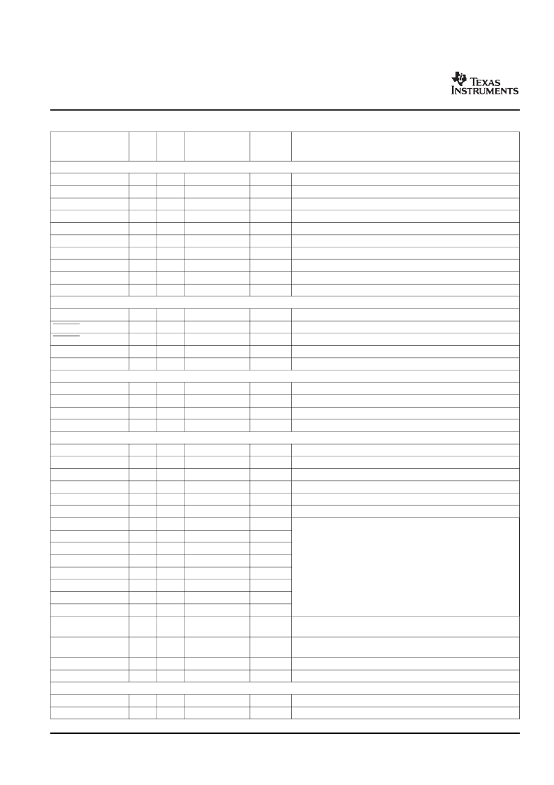
Table 2-4. TERMINAL FUNCTIONS (continued)
TERMINAL NAME
NO
TYPE
INTERNAL
PULLUP/
PULLDOWN
OPER
VOLT
DESCRIPTION
SGMII0/1 and MDIO
1.2 V
1.2 V
1.2 V
1.2 V
1.2 V
1.2 V
1.2 V
1.2 V
3.3 V
3.3 V
SPI or UART
3.3 V
3.3 V
3.3 V
3.3 V
3.3 V
TIMER 0/1 or GPIO[8:11]
3.3 V
3.3 V
3.3 V
3.3 V
MCASP OR VIDEO PORT OR VIC
3.3 V
3.3 V
3.3 V
3.3 V
3.3 V
3.3 V
3.3 V
3.3 V
3.3 V
3.3 V
3.3 V
3.3 V
3.3 V
3.3 V
3.3 V
SGMII0RXN
SGMII0RXP
SGMII0TXN
SGMII0TXP
SGMII1RXN
SGMII1RXP
SGMII1TXN
SGMII1TXP
MDCLK
MDIO
AA10
AA9
W11
Y11
AC9
AB9
W9
W8
U9
U8
I
I
Differential SGMII port 0 RX input (negative)
Differential SGMII port 0 RX input (positive)
Differential SGMII port 0 TX output (negative)
Differential SGMII port 0 TX output (positive)
Differential SGMII port 1 RX input (negative)
Differential SGMII port 1 RX input (positive)
Differential SGMII port 1 TX output (negative)
Differential SGMII port 1 TX output (positive)
MDIO serial clock (MDCLK)
MDIO serial data (MDIO)
O
O
I
I
O
O
OZ
I/O/Z
IPD
IPU
SPICLK
SPICS1/UARTTX
SPICS2/UARTRX
SPIDI/UARTRTS
SPIDO/UARTCTS
F22
D23
F23
G23
F21
I/O/Z
I/O/Z
I/O/Z
I/O/Z
I/O/Z
IPU
IPU
IPU
IPU
IPU
SPI clock output
SPI chip select 1 or UART transmit (O/Z)
SPI chip select 2 or UART receive
SPI data input or UART ready to send (O/Z)
SPI data output or UART clear to send
T0INP12/GP08
T0OUT12/GP09
T1INP12/GP10
T1OUT12/GP11
E20
D21
E21
C22
I/O/Z
I/O/Z
I/O/Z
I/O/Z
IPD
IPD
IPD
IPD
Timer 0 input pin for lower 32-bit counter (I) or GPIO 8
Timer 0 output pin for lower 32-bit counter (O/Z) or GPIO 9
Timer 1 input pin for lower 32-bit counter (I) or GPIO 10
Timer 1 output pin for lower 32-bit counter(O/Z) or GPIO 11
AHCLKR
AHCLKX
ACLKR
ACLKX
AFSR
AFSX
AXR0
AXR1
AXR2
AXR3
AXR4
AXR5
AXR6
AXR7
STCLK/AXR8
AC4
AC3
AC6
AC7
W6
AA7
AB6
Y6
AA6
AB4
Y5
V7
AA4
V6
Y7
I/O/Z
I/O/Z
I/O/Z
I/O/Z
I/O/Z
I/O/Z
I/O/Z
IPD
IPD
IPD
IPD
IPD
IPD
IPD
IPD
IPD
IPD
IPD
IPD
IPD
IPD
IPD
McASP receive high-frequency master clock
McASP transmit high-frequency master clock
McASP receive master clock
McASP transmit master clock
McASP receive frame sync or left/right clock (LRCLK)
McASP transmit frame sync or left/right clock (LRCLK)
McASP data pin [0:7]
I/O/Z
The STCLK signal drives the hardware counter for use by the
video ports (I) or McASP data pin 8.
VCXO Interpolated Control Port (VIC) single-bit digital-to-analog
converter(VDAC) output (O) or McASP data pin 9
McASP mute input
McASP mute output (O/Z).
VIDEO PORT 0 OR GPIO[12:15]
3.3 V
Video Port 0 Clock 0 (I)
3.3 V
Video Port 0 Clock 1
VDAC/AXR9
AA5
I/O/Z
IPD
3.3 V
AMUTEIN
AMUTE
AB3
U7
I/O/Z
I/O/Z
IPD
IPD
3.3 V
3.3 V
VP0CLK0
VP0CLK1
Y23
V23
I
IPU
IPU
I/O/Z
Device Overview
24
Submit Documentation Feedback
相關(guān)PDF資料 |
PDF描述 |
|---|---|
| TMX320DM647ZUT900 | Digital Media Processor |
| TMX320DM648ZUT720 | Digital Media Processor |
| TMX320DM648ZUT900 | Digital Media Processor |
| TMS320LC31PQL | DIGITAL SIGNAL PROCESSORS |
| TMX320C6414TGLZ | FIXED-POINT DIGITAL SIGNAL PROCESSORS |
相關(guān)代理商/技術(shù)參數(shù) |
參數(shù)描述 |
|---|---|
| TMX320DM647ZUT900 | 制造商:TI 制造商全稱:Texas Instruments 功能描述:Digital Media Processor |
| TMX320DM648ACUT7 | 制造商:Texas Instruments 功能描述:- Trays |
| TMX320DM648ACUT9 | 制造商:Texas Instruments 功能描述:- Trays |
| TMX320DM648AZUT7 | 制造商:Texas Instruments 功能描述: |
| TMX320DM648CUT7 | 制造商:Texas Instruments 功能描述:- Trays |
發(fā)布緊急采購(gòu),3分鐘左右您將得到回復(fù)。