- 您現(xiàn)在的位置:買(mǎi)賣(mài)IC網(wǎng) > PDF目錄383961 > TMX320DM647ZUT720 (Texas Instruments, Inc.) Digital Media Processor PDF資料下載
參數(shù)資料
| 型號(hào): | TMX320DM647ZUT720 |
| 廠商: | Texas Instruments, Inc. |
| 英文描述: | Digital Media Processor |
| 中文描述: | 數(shù)字媒體處理器 |
| 文件頁(yè)數(shù): | 27/166頁(yè) |
| 文件大?。?/td> | 1341K |
| 代理商: | TMX320DM647ZUT720 |
第1頁(yè)第2頁(yè)第3頁(yè)第4頁(yè)第5頁(yè)第6頁(yè)第7頁(yè)第8頁(yè)第9頁(yè)第10頁(yè)第11頁(yè)第12頁(yè)第13頁(yè)第14頁(yè)第15頁(yè)第16頁(yè)第17頁(yè)第18頁(yè)第19頁(yè)第20頁(yè)第21頁(yè)第22頁(yè)第23頁(yè)第24頁(yè)第25頁(yè)第26頁(yè)當(dāng)前第27頁(yè)第28頁(yè)第29頁(yè)第30頁(yè)第31頁(yè)第32頁(yè)第33頁(yè)第34頁(yè)第35頁(yè)第36頁(yè)第37頁(yè)第38頁(yè)第39頁(yè)第40頁(yè)第41頁(yè)第42頁(yè)第43頁(yè)第44頁(yè)第45頁(yè)第46頁(yè)第47頁(yè)第48頁(yè)第49頁(yè)第50頁(yè)第51頁(yè)第52頁(yè)第53頁(yè)第54頁(yè)第55頁(yè)第56頁(yè)第57頁(yè)第58頁(yè)第59頁(yè)第60頁(yè)第61頁(yè)第62頁(yè)第63頁(yè)第64頁(yè)第65頁(yè)第66頁(yè)第67頁(yè)第68頁(yè)第69頁(yè)第70頁(yè)第71頁(yè)第72頁(yè)第73頁(yè)第74頁(yè)第75頁(yè)第76頁(yè)第77頁(yè)第78頁(yè)第79頁(yè)第80頁(yè)第81頁(yè)第82頁(yè)第83頁(yè)第84頁(yè)第85頁(yè)第86頁(yè)第87頁(yè)第88頁(yè)第89頁(yè)第90頁(yè)第91頁(yè)第92頁(yè)第93頁(yè)第94頁(yè)第95頁(yè)第96頁(yè)第97頁(yè)第98頁(yè)第99頁(yè)第100頁(yè)第101頁(yè)第102頁(yè)第103頁(yè)第104頁(yè)第105頁(yè)第106頁(yè)第107頁(yè)第108頁(yè)第109頁(yè)第110頁(yè)第111頁(yè)第112頁(yè)第113頁(yè)第114頁(yè)第115頁(yè)第116頁(yè)第117頁(yè)第118頁(yè)第119頁(yè)第120頁(yè)第121頁(yè)第122頁(yè)第123頁(yè)第124頁(yè)第125頁(yè)第126頁(yè)第127頁(yè)第128頁(yè)第129頁(yè)第130頁(yè)第131頁(yè)第132頁(yè)第133頁(yè)第134頁(yè)第135頁(yè)第136頁(yè)第137頁(yè)第138頁(yè)第139頁(yè)第140頁(yè)第141頁(yè)第142頁(yè)第143頁(yè)第144頁(yè)第145頁(yè)第146頁(yè)第147頁(yè)第148頁(yè)第149頁(yè)第150頁(yè)第151頁(yè)第152頁(yè)第153頁(yè)第154頁(yè)第155頁(yè)第156頁(yè)第157頁(yè)第158頁(yè)第159頁(yè)第160頁(yè)第161頁(yè)第162頁(yè)第163頁(yè)第164頁(yè)第165頁(yè)第166頁(yè)
www.ti.com
P
TMS320DM647/TMS320DM648
Digital Media Processor
SPRS372–MAY 2007
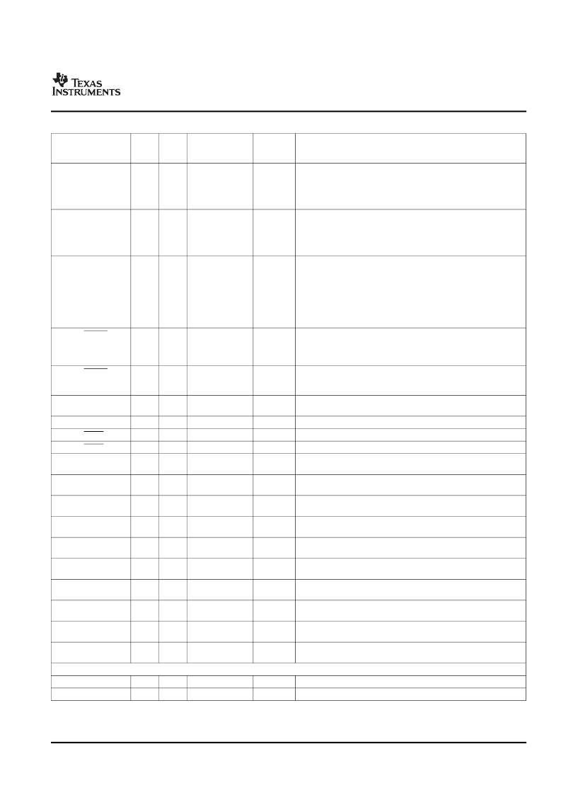
Table 2-4. TERMINAL FUNCTIONS (continued)
TERMINAL NAME
NO
TYPE
INTERNAL
PULLUP/
PULLDOWN
IPD
OPER
VOLT
DESCRIPTION
VP4CTL0/ABA0
J2
I/O/Z
3.3 V
Video Port 4 Control 0 or EMIFA bank address control (ABA[1:0])
(O/Z). Active-low bank selects for the 16-bit EMIFA. When
interfacing to 16-bit asynchronous devices, ABA1 carries bit 1 of
the byte address. For an 8-bit asynchronous interface, ABA[1:0]
are used to carry bits 1 and 0 of the byte address.
Video Port 4 Control 1 or EMIFA bank address control (ABA[1:0])
(O/Z). Active-low bank selects for the 16-bit EMIFA. WHEN
interfacing to 16-bit asynchronous devices, ABA1 carries bit 1 of
the byte address. For an 8-bit asynchronous interface, ABA[1:0]
are used to carry bits 1 and 0 of the byte address.
Video Port 4 Control 2 or Programmable synchronous address
strobe or read-enable. For programmable synchronous interface,
the r_enable field in the ChipSelect x Configuration Register
selects between ASADS and ASRE:
– If r_enable = 0, then the ASADS/ASRE signal functions as the
ASADS signal.
– If r_enable = 1, then the ASADS/ASRE signal functions as the
ASRE signal.
Video Port 4 Data 2 or EMIFA byte-enable control 0. Decoded
from the low-order address bits. The number of address bits or
byte enables used depends on the width of external memory.
Byte-write enables for most types of memory.
Video Port 4 Data 3 or EMIFA byte-enable control 1. Number of
address bits or byte enables used depends on the width of
external memory. Byte-write enables for most types of memory.
Video Port 4 Data 4 or EMIFA External Address 10 (word address)
(O/Z)
Video Port 4 Data 5
Video Port 4 Data 6 or EMIFA memory space enable 2
Video Port 4 Data 7 or EMIFA memory space enable 3
Video Port 4 Data 8 or EMIFA External Address 0 (word address)
(O/Z)
Video Port 4 Data 9 or EMIFA External Address 1 (word address)
(O/Z)
Video Port 4 Data 12 or EMIFA External Address 2 (word address)
(O/Z)
Video Port 4 Data 13 or EMIFA External Address 3 (word address)
(O/Z)
Video Port 4 Data 14 or EMIFA External Address 4 (word address)
(O/Z)
Video Port 4 Data 15 or EMIFA External Address 5 (word address)
(O/Z)
Video Port 4 Data 16 or EMIFA External Address 6 (word address)
(O/Z)
Video Port 4 Data 17 or EMIFA External Address 7 (word address)
(O/Z)
Video Port 4 Data 18 or EMIFA External Address 8 (word address)
(O/Z)
Video Port 4 Data 19 or EMIFA External Address 9 (word address)
(O/Z)
EMIFA
3.3 V
EMIFA External Address 23 (word address) (O/Z)
3.3 V
EMIFA External Address 19 (word address) (O/Z)
VP4CTL1/ABA1
J1
I/O/Z
IPD
3.3 V
VP4CTL2/AADS
K2
I/O/Z
IPD
3.3 V
VP4D02/ABE00
L2
I/O/Z
IPU
3.3 V
VP4D03/ABE01
M4
I/O/Z
IPU
3.3 V
VP4D04/AEA10
M5
I/O/Z
IPU
3.3 V
VP4D05
VP4D06/ACE2
VP4D07/ACE3
VP4D08/AEA00
M6
L3
L4
L5
I/O/Z
I/O/Z
I/O/Z
I/O/Z
IPU
IPU
IPU
IPD
3.3 V
3.3 V
3.3 V
3.3 V
VP4D09/AEA01
K3
I/O/Z
IPD
3.3 V
VP4D12/AEA02
K4
I/O/Z
IPD
3.3 V
VP4D13/AEA03
L6
I/O/Z
IPD
3.3 V
VP4D14/AEA04
K5
I/O/Z
IPD
3.3 V
VP4D15/AEA05
J3
I/O/Z
IPD
3.3 V
VP4D16/AEA06
J4
I/O/Z
IPD
3.3 V
VP4D17/AEA07
J5
I/O/Z
IPD
3.3 V
VP4D18/AEA08
J6
I/O/Z
IPD
3.3 V
VP4D19/AEA09
K6
I/O/Z
IPD
3.3 V
AEA23
AEA19
H4
H5
OZ
I/O/Z
IPD
IPU
Submit Documentation Feedback
Device Overview
27
相關(guān)PDF資料 |
PDF描述 |
|---|---|
| TMX320DM647ZUT900 | Digital Media Processor |
| TMX320DM648ZUT720 | Digital Media Processor |
| TMX320DM648ZUT900 | Digital Media Processor |
| TMS320LC31PQL | DIGITAL SIGNAL PROCESSORS |
| TMX320C6414TGLZ | FIXED-POINT DIGITAL SIGNAL PROCESSORS |
相關(guān)代理商/技術(shù)參數(shù) |
參數(shù)描述 |
|---|---|
| TMX320DM647ZUT900 | 制造商:TI 制造商全稱(chēng):Texas Instruments 功能描述:Digital Media Processor |
| TMX320DM648ACUT7 | 制造商:Texas Instruments 功能描述:- Trays |
| TMX320DM648ACUT9 | 制造商:Texas Instruments 功能描述:- Trays |
| TMX320DM648AZUT7 | 制造商:Texas Instruments 功能描述: |
| TMX320DM648CUT7 | 制造商:Texas Instruments 功能描述:- Trays |
發(fā)布緊急采購(gòu),3分鐘左右您將得到回復(fù)。