- 您現(xiàn)在的位置:買(mǎi)賣(mài)IC網(wǎng) > PDF目錄98068 > S1C38000B0A0100 32-BIT, RISC MICROCONTROLLER, BGA239 PDF資料下載
參數(shù)資料
| 型號(hào): | S1C38000B0A0100 |
| 元件分類(lèi): | 微控制器/微處理器 |
| 英文描述: | 32-BIT, RISC MICROCONTROLLER, BGA239 |
| 封裝: | CFLGA-239 |
| 文件頁(yè)數(shù): | 195/281頁(yè) |
| 文件大?。?/td> | 1309K |
| 代理商: | S1C38000B0A0100 |
第1頁(yè)第2頁(yè)第3頁(yè)第4頁(yè)第5頁(yè)第6頁(yè)第7頁(yè)第8頁(yè)第9頁(yè)第10頁(yè)第11頁(yè)第12頁(yè)第13頁(yè)第14頁(yè)第15頁(yè)第16頁(yè)第17頁(yè)第18頁(yè)第19頁(yè)第20頁(yè)第21頁(yè)第22頁(yè)第23頁(yè)第24頁(yè)第25頁(yè)第26頁(yè)第27頁(yè)第28頁(yè)第29頁(yè)第30頁(yè)第31頁(yè)第32頁(yè)第33頁(yè)第34頁(yè)第35頁(yè)第36頁(yè)第37頁(yè)第38頁(yè)第39頁(yè)第40頁(yè)第41頁(yè)第42頁(yè)第43頁(yè)第44頁(yè)第45頁(yè)第46頁(yè)第47頁(yè)第48頁(yè)第49頁(yè)第50頁(yè)第51頁(yè)第52頁(yè)第53頁(yè)第54頁(yè)第55頁(yè)第56頁(yè)第57頁(yè)第58頁(yè)第59頁(yè)第60頁(yè)第61頁(yè)第62頁(yè)第63頁(yè)第64頁(yè)第65頁(yè)第66頁(yè)第67頁(yè)第68頁(yè)第69頁(yè)第70頁(yè)第71頁(yè)第72頁(yè)第73頁(yè)第74頁(yè)第75頁(yè)第76頁(yè)第77頁(yè)第78頁(yè)第79頁(yè)第80頁(yè)第81頁(yè)第82頁(yè)第83頁(yè)第84頁(yè)第85頁(yè)第86頁(yè)第87頁(yè)第88頁(yè)第89頁(yè)第90頁(yè)第91頁(yè)第92頁(yè)第93頁(yè)第94頁(yè)第95頁(yè)第96頁(yè)第97頁(yè)第98頁(yè)第99頁(yè)第100頁(yè)第101頁(yè)第102頁(yè)第103頁(yè)第104頁(yè)第105頁(yè)第106頁(yè)第107頁(yè)第108頁(yè)第109頁(yè)第110頁(yè)第111頁(yè)第112頁(yè)第113頁(yè)第114頁(yè)第115頁(yè)第116頁(yè)第117頁(yè)第118頁(yè)第119頁(yè)第120頁(yè)第121頁(yè)第122頁(yè)第123頁(yè)第124頁(yè)第125頁(yè)第126頁(yè)第127頁(yè)第128頁(yè)第129頁(yè)第130頁(yè)第131頁(yè)第132頁(yè)第133頁(yè)第134頁(yè)第135頁(yè)第136頁(yè)第137頁(yè)第138頁(yè)第139頁(yè)第140頁(yè)第141頁(yè)第142頁(yè)第143頁(yè)第144頁(yè)第145頁(yè)第146頁(yè)第147頁(yè)第148頁(yè)第149頁(yè)第150頁(yè)第151頁(yè)第152頁(yè)第153頁(yè)第154頁(yè)第155頁(yè)第156頁(yè)第157頁(yè)第158頁(yè)第159頁(yè)第160頁(yè)第161頁(yè)第162頁(yè)第163頁(yè)第164頁(yè)第165頁(yè)第166頁(yè)第167頁(yè)第168頁(yè)第169頁(yè)第170頁(yè)第171頁(yè)第172頁(yè)第173頁(yè)第174頁(yè)第175頁(yè)第176頁(yè)第177頁(yè)第178頁(yè)第179頁(yè)第180頁(yè)第181頁(yè)第182頁(yè)第183頁(yè)第184頁(yè)第185頁(yè)第186頁(yè)第187頁(yè)第188頁(yè)第189頁(yè)第190頁(yè)第191頁(yè)第192頁(yè)第193頁(yè)第194頁(yè)當(dāng)前第195頁(yè)第196頁(yè)第197頁(yè)第198頁(yè)第199頁(yè)第200頁(yè)第201頁(yè)第202頁(yè)第203頁(yè)第204頁(yè)第205頁(yè)第206頁(yè)第207頁(yè)第208頁(yè)第209頁(yè)第210頁(yè)第211頁(yè)第212頁(yè)第213頁(yè)第214頁(yè)第215頁(yè)第216頁(yè)第217頁(yè)第218頁(yè)第219頁(yè)第220頁(yè)第221頁(yè)第222頁(yè)第223頁(yè)第224頁(yè)第225頁(yè)第226頁(yè)第227頁(yè)第228頁(yè)第229頁(yè)第230頁(yè)第231頁(yè)第232頁(yè)第233頁(yè)第234頁(yè)第235頁(yè)第236頁(yè)第237頁(yè)第238頁(yè)第239頁(yè)第240頁(yè)第241頁(yè)第242頁(yè)第243頁(yè)第244頁(yè)第245頁(yè)第246頁(yè)第247頁(yè)第248頁(yè)第249頁(yè)第250頁(yè)第251頁(yè)第252頁(yè)第253頁(yè)第254頁(yè)第255頁(yè)第256頁(yè)第257頁(yè)第258頁(yè)第259頁(yè)第260頁(yè)第261頁(yè)第262頁(yè)第263頁(yè)第264頁(yè)第265頁(yè)第266頁(yè)第267頁(yè)第268頁(yè)第269頁(yè)第270頁(yè)第271頁(yè)第272頁(yè)第273頁(yè)第274頁(yè)第275頁(yè)第276頁(yè)第277頁(yè)第278頁(yè)第279頁(yè)第280頁(yè)第281頁(yè)
28 COMPACTFLASH
260
EPSON
S1C38000 TECHNICAL MANUAL
28 CompactFlash
28.1 Overview
The S1C38000 provides a 3.3V interface for a single CompactFlash (CF) card device. To interface
to a 5V CompactFlash device, external level shifting and isolation buffers are required. For both
3.3V and 5V devices, isolation buffers and transceivers must be used on the address bus and data
bus respectively. Two additional output signals to control the external buffers and transceivers are
provided: CFDEN# as the address and data enable for the address buffer and the data transceiver,
and CFDDIR as the data direction control for the data transceiver. These two output pins can be re-
configured to GPO pins if CompactFlash support is not needed. This re-configuration bit resides in
the GPIO Port registers.
Memory mode and I/O modes are supported; True IDE mode is not supported.
28.2 Register Descriptions
The default base address for the CF registers is F8000C00h. All non-reserved register bits default to
0 unless specified otherwise.
<Read>
1
Input-caused interrupt from CompactFlash
0
No interrupt (default)
<Write>
1
Clear interrupt bit
0
No change
bit 15
CFWP OUT
Negative interrupt on active high, memory mode write protect pin, CFWP1.
bit 14
CFREADY OUT
Negative interrupt on active high, memory mode ready pin, CFREADY1.
bits 13–12 CFBVD[2:1] OUT
Negative interrupt on active high, battery voltage detect pins, CFBVD[2:1]1.
bits 11–10 CFVS[2:1]# OUT
Positive interrupt on active low, voltage sense pins, CFVS[2:1]#2.
bits 9–8
CFCD[2:1]# OUT
Positive interrupt on active low, card detect pins, CFCD[2:1]#3.
bit 7
CFWP IN
Positive interrupt on active high, memory mode write protect pin, CFWP1.
bit 6
CFREADY IN
Positive interrupt on active high, memory mode ready pin, CFREADY1.
bits 5–4
CFBVD[2:1] IN
Positive interrupt on active high, battery voltage detect pins, CFBVD[2:1]1.
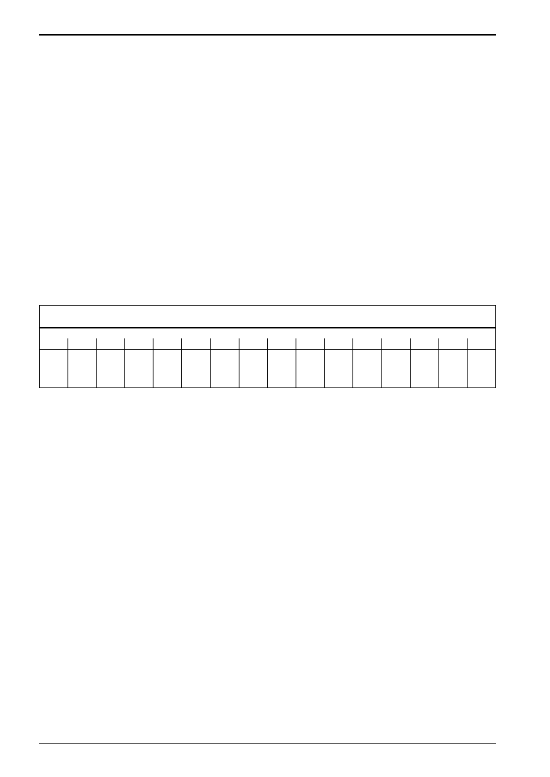
CompactFlash Input Interrupt Status/Clear Register
CF[00h]
Default = 0000 0000h
Read/Write
n/a
31
30
29
28
27
26
25
24
23
22
21
20
19
18
17
16
CFWP
Inactive
(Input)
CFREADY
Inactive
(Input)
CFBVD2
Inactive
(Input)
CFBVD1
Inactive
(Input)
CFVS2#
Inactive
(Input)
CFVS1#
Inactive
(Input)
CFCD2#
High
(Input)
CFCD1#
High
(Input)
CFWP
Active
(Input)
CFREADY
Active
(Input)
CFBVD2
Active
(Input)
CFBVD1
Active
(Input)
CFVS2#
Active
(Input)
CFVS1#
Active
(Input)
CFCD2#
Low
(Input)
CFCD1#
Low
(Input)
15
14
13
12
11
10
9876543210
相關(guān)PDF資料 |
PDF描述 |
|---|---|
| S1C60L02F | 4-BIT, MROM, 0.08 MHz, MICROCONTROLLER, PQFP60 |
| S1C60L05F | 4-BIT, MROM, 0.08 MHz, MICROCONTROLLER, PQFP60 |
| S1C60L05D | 4-BIT, MROM, 0.08 MHz, MICROCONTROLLER, UUC53 |
| S1C60L13F | 4-BIT, MROM, 0.032768 MHz, MICROCONTROLLER, PQFP80 |
| S1C60L13D | 4-BIT, MROM, 0.032768 MHz, MICROCONTROLLER, UUC79 |
相關(guān)代理商/技術(shù)參數(shù) |
參數(shù)描述 |
|---|---|
| S1C-38-S | 制造商:GRIPCO 功能描述: |
| S-1-C-6.6-D D/C .670 OAL | 功能描述:觸點(diǎn)探頭 HEADLESS FLAT RoHS:否 制造商:IDI 類(lèi)型:Probes 尖端類(lèi)型:Spherical Radius 長(zhǎng)度:8.26 mm 電流額定值:10 A 彈力:2.3 oz 行程:1.52 mm 系列:101050 |
| S-1-C-6.6-G D/C .670 OAL | 功能描述:觸點(diǎn)探頭 HEADLESS FLAT RoHS:否 制造商:IDI 類(lèi)型:Probes 尖端類(lèi)型:Spherical Radius 長(zhǎng)度:8.26 mm 電流額定值:10 A 彈力:2.3 oz 行程:1.52 mm 系列:101050 |
| S1C60A08 | 制造商:EPSON 制造商全稱(chēng):EPSON 功能描述:4-bit Single Chip Microcomputer |
| S1C60A16 | 制造商:EPSON 制造商全稱(chēng):EPSON 功能描述:4-bit Single Chip Microcomputer |
發(fā)布緊急采購(gòu),3分鐘左右您將得到回復(fù)。