- 您現(xiàn)在的位置:買賣IC網(wǎng) > PDF目錄98068 > S1C38000B0A0100 32-BIT, RISC MICROCONTROLLER, BGA239 PDF資料下載
參數(shù)資料
| 型號(hào): | S1C38000B0A0100 |
| 元件分類: | 微控制器/微處理器 |
| 英文描述: | 32-BIT, RISC MICROCONTROLLER, BGA239 |
| 封裝: | CFLGA-239 |
| 文件頁(yè)數(shù): | 16/281頁(yè) |
| 文件大小: | 1309K |
| 代理商: | S1C38000B0A0100 |
第1頁(yè)第2頁(yè)第3頁(yè)第4頁(yè)第5頁(yè)第6頁(yè)第7頁(yè)第8頁(yè)第9頁(yè)第10頁(yè)第11頁(yè)第12頁(yè)第13頁(yè)第14頁(yè)第15頁(yè)當(dāng)前第16頁(yè)第17頁(yè)第18頁(yè)第19頁(yè)第20頁(yè)第21頁(yè)第22頁(yè)第23頁(yè)第24頁(yè)第25頁(yè)第26頁(yè)第27頁(yè)第28頁(yè)第29頁(yè)第30頁(yè)第31頁(yè)第32頁(yè)第33頁(yè)第34頁(yè)第35頁(yè)第36頁(yè)第37頁(yè)第38頁(yè)第39頁(yè)第40頁(yè)第41頁(yè)第42頁(yè)第43頁(yè)第44頁(yè)第45頁(yè)第46頁(yè)第47頁(yè)第48頁(yè)第49頁(yè)第50頁(yè)第51頁(yè)第52頁(yè)第53頁(yè)第54頁(yè)第55頁(yè)第56頁(yè)第57頁(yè)第58頁(yè)第59頁(yè)第60頁(yè)第61頁(yè)第62頁(yè)第63頁(yè)第64頁(yè)第65頁(yè)第66頁(yè)第67頁(yè)第68頁(yè)第69頁(yè)第70頁(yè)第71頁(yè)第72頁(yè)第73頁(yè)第74頁(yè)第75頁(yè)第76頁(yè)第77頁(yè)第78頁(yè)第79頁(yè)第80頁(yè)第81頁(yè)第82頁(yè)第83頁(yè)第84頁(yè)第85頁(yè)第86頁(yè)第87頁(yè)第88頁(yè)第89頁(yè)第90頁(yè)第91頁(yè)第92頁(yè)第93頁(yè)第94頁(yè)第95頁(yè)第96頁(yè)第97頁(yè)第98頁(yè)第99頁(yè)第100頁(yè)第101頁(yè)第102頁(yè)第103頁(yè)第104頁(yè)第105頁(yè)第106頁(yè)第107頁(yè)第108頁(yè)第109頁(yè)第110頁(yè)第111頁(yè)第112頁(yè)第113頁(yè)第114頁(yè)第115頁(yè)第116頁(yè)第117頁(yè)第118頁(yè)第119頁(yè)第120頁(yè)第121頁(yè)第122頁(yè)第123頁(yè)第124頁(yè)第125頁(yè)第126頁(yè)第127頁(yè)第128頁(yè)第129頁(yè)第130頁(yè)第131頁(yè)第132頁(yè)第133頁(yè)第134頁(yè)第135頁(yè)第136頁(yè)第137頁(yè)第138頁(yè)第139頁(yè)第140頁(yè)第141頁(yè)第142頁(yè)第143頁(yè)第144頁(yè)第145頁(yè)第146頁(yè)第147頁(yè)第148頁(yè)第149頁(yè)第150頁(yè)第151頁(yè)第152頁(yè)第153頁(yè)第154頁(yè)第155頁(yè)第156頁(yè)第157頁(yè)第158頁(yè)第159頁(yè)第160頁(yè)第161頁(yè)第162頁(yè)第163頁(yè)第164頁(yè)第165頁(yè)第166頁(yè)第167頁(yè)第168頁(yè)第169頁(yè)第170頁(yè)第171頁(yè)第172頁(yè)第173頁(yè)第174頁(yè)第175頁(yè)第176頁(yè)第177頁(yè)第178頁(yè)第179頁(yè)第180頁(yè)第181頁(yè)第182頁(yè)第183頁(yè)第184頁(yè)第185頁(yè)第186頁(yè)第187頁(yè)第188頁(yè)第189頁(yè)第190頁(yè)第191頁(yè)第192頁(yè)第193頁(yè)第194頁(yè)第195頁(yè)第196頁(yè)第197頁(yè)第198頁(yè)第199頁(yè)第200頁(yè)第201頁(yè)第202頁(yè)第203頁(yè)第204頁(yè)第205頁(yè)第206頁(yè)第207頁(yè)第208頁(yè)第209頁(yè)第210頁(yè)第211頁(yè)第212頁(yè)第213頁(yè)第214頁(yè)第215頁(yè)第216頁(yè)第217頁(yè)第218頁(yè)第219頁(yè)第220頁(yè)第221頁(yè)第222頁(yè)第223頁(yè)第224頁(yè)第225頁(yè)第226頁(yè)第227頁(yè)第228頁(yè)第229頁(yè)第230頁(yè)第231頁(yè)第232頁(yè)第233頁(yè)第234頁(yè)第235頁(yè)第236頁(yè)第237頁(yè)第238頁(yè)第239頁(yè)第240頁(yè)第241頁(yè)第242頁(yè)第243頁(yè)第244頁(yè)第245頁(yè)第246頁(yè)第247頁(yè)第248頁(yè)第249頁(yè)第250頁(yè)第251頁(yè)第252頁(yè)第253頁(yè)第254頁(yè)第255頁(yè)第256頁(yè)第257頁(yè)第258頁(yè)第259頁(yè)第260頁(yè)第261頁(yè)第262頁(yè)第263頁(yè)第264頁(yè)第265頁(yè)第266頁(yè)第267頁(yè)第268頁(yè)第269頁(yè)第270頁(yè)第271頁(yè)第272頁(yè)第273頁(yè)第274頁(yè)第275頁(yè)第276頁(yè)第277頁(yè)第278頁(yè)第279頁(yè)第280頁(yè)第281頁(yè)
11 POWER MANAGER
98
EPSON
S1C38000 TECHNICAL MANUAL
11 Power Manager
11.1 Overview
The Power Manager serves several functions. One function is to control the source and frequency of
the various internal clocks of the S1C38000. Other functions of the Power Manager are to manage
the power down modes of the S1C38000, and to generate the internal system reset based on the
RESET# input pin or the watchdog timer reset signal.
11.2 PLL Configuration
The S1C38000 has two internal PLL’s, one of which requires a 32.768 kHz reference clock source.
The other PLL is optional and requires a 6 MHz reference clock source. Both PLL’s are designed to
use crystal inputs for the reference clock.
The 32.768 kHz PLL (PLLA) has one output clock (POUTA) which has a default multiplier value at
reset to generate a 48 MHz clock. POUTA may be used to generate the pixel clock to the LCDC
where a flexible pixel clock rate may be needed.
The 6 MHz PLL (PLLB) is optional and provides the USB and FIR modules with a very accurate 48
MHz clock.
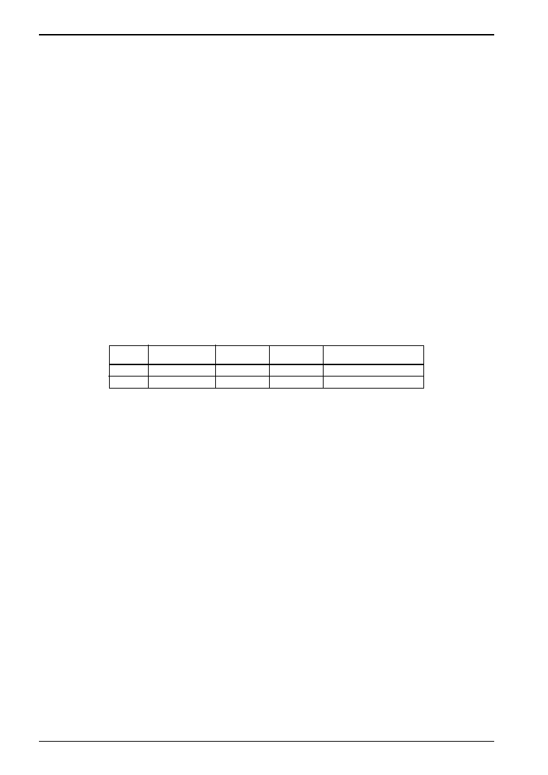
Table 11-1 describes the various possible PLL output clock frequencies.
11.3 Internal Clocks
There are six main internal clocks in the S1C38000:
BUSCLK - Bus clock for the AHB/APB bus. BUSCLK is also used as the CPU clock for the
ARM720T in synchronous CPU mode.
CPUCLK - CPU clock for the ARM720T in asynchronous CPU mode. CPUCLK is not used in
synchronous CPU mode.
The MD1 System Configuration pin allows the ARM720T to run in a synchronous CPU mode or
an asynchronous CPU mode. Synchronous CPU mode is when the CPU and the system bus are
running from the same clock source. Asynchronous CPU mode is when the CPU is running at a
higher frequency than the system bus. MD2 specifies the clock frequency for the CPU in this
mode.
RTCLK - Clock source for the Real Time Clock module and for other modules where a slow
clock is required for certain functions (i.e., SDRAM refresh). RTCLK should always be 32.768
kHz under normal operation.
USBCLK - Clock source for the USB module. USBCLK should always be 48 MHz under normal
operation.
LCDCLK - Clock source for the LCDC pixel clock.
UARTCLK - 24 MHz clock source for the UARTs and Timers.
Figure 11-1 shows the routing paths for all six internal clocks. Note that some routing paths are used
for test mode only and are never used for normal operation.
Table 11-1 PLL Output Clocks Configuration
PLL
Reference Clock
Frequency
PLL Multiplier
Value
PLL VCO
Clock
PLL Output Clocks
PLLA
32.768 kHz
x 2930
POUTA x 2
POUTA = 48.00512 MHz
PLLB
6 MHz
x 8
POUTB x 2
POUTB = 48 MHz
相關(guān)PDF資料 |
PDF描述 |
|---|---|
| S1C60L02F | 4-BIT, MROM, 0.08 MHz, MICROCONTROLLER, PQFP60 |
| S1C60L05F | 4-BIT, MROM, 0.08 MHz, MICROCONTROLLER, PQFP60 |
| S1C60L05D | 4-BIT, MROM, 0.08 MHz, MICROCONTROLLER, UUC53 |
| S1C60L13F | 4-BIT, MROM, 0.032768 MHz, MICROCONTROLLER, PQFP80 |
| S1C60L13D | 4-BIT, MROM, 0.032768 MHz, MICROCONTROLLER, UUC79 |
相關(guān)代理商/技術(shù)參數(shù) |
參數(shù)描述 |
|---|---|
| S1C-38-S | 制造商:GRIPCO 功能描述: |
| S-1-C-6.6-D D/C .670 OAL | 功能描述:觸點(diǎn)探頭 HEADLESS FLAT RoHS:否 制造商:IDI 類型:Probes 尖端類型:Spherical Radius 長(zhǎng)度:8.26 mm 電流額定值:10 A 彈力:2.3 oz 行程:1.52 mm 系列:101050 |
| S-1-C-6.6-G D/C .670 OAL | 功能描述:觸點(diǎn)探頭 HEADLESS FLAT RoHS:否 制造商:IDI 類型:Probes 尖端類型:Spherical Radius 長(zhǎng)度:8.26 mm 電流額定值:10 A 彈力:2.3 oz 行程:1.52 mm 系列:101050 |
| S1C60A08 | 制造商:EPSON 制造商全稱:EPSON 功能描述:4-bit Single Chip Microcomputer |
| S1C60A16 | 制造商:EPSON 制造商全稱:EPSON 功能描述:4-bit Single Chip Microcomputer |
發(fā)布緊急采購(gòu),3分鐘左右您將得到回復(fù)。