- 您現(xiàn)在的位置:買賣IC網(wǎng) > PDF目錄379804 > CD2481 (Intel Corp.) Programmable Four-Channel Communications Controller PDF資料下載
參數(shù)資料
| 型號(hào): | CD2481 |
| 廠商: | Intel Corp. |
| 英文描述: | Programmable Four-Channel Communications Controller |
| 中文描述: | 可編程四通道通信控制器 |
| 文件頁數(shù): | 19/222頁 |
| 文件大?。?/td> | 974K |
| 代理商: | CD2481 |
第1頁第2頁第3頁第4頁第5頁第6頁第7頁第8頁第9頁第10頁第11頁第12頁第13頁第14頁第15頁第16頁第17頁第18頁當(dāng)前第19頁第20頁第21頁第22頁第23頁第24頁第25頁第26頁第27頁第28頁第29頁第30頁第31頁第32頁第33頁第34頁第35頁第36頁第37頁第38頁第39頁第40頁第41頁第42頁第43頁第44頁第45頁第46頁第47頁第48頁第49頁第50頁第51頁第52頁第53頁第54頁第55頁第56頁第57頁第58頁第59頁第60頁第61頁第62頁第63頁第64頁第65頁第66頁第67頁第68頁第69頁第70頁第71頁第72頁第73頁第74頁第75頁第76頁第77頁第78頁第79頁第80頁第81頁第82頁第83頁第84頁第85頁第86頁第87頁第88頁第89頁第90頁第91頁第92頁第93頁第94頁第95頁第96頁第97頁第98頁第99頁第100頁第101頁第102頁第103頁第104頁第105頁第106頁第107頁第108頁第109頁第110頁第111頁第112頁第113頁第114頁第115頁第116頁第117頁第118頁第119頁第120頁第121頁第122頁第123頁第124頁第125頁第126頁第127頁第128頁第129頁第130頁第131頁第132頁第133頁第134頁第135頁第136頁第137頁第138頁第139頁第140頁第141頁第142頁第143頁第144頁第145頁第146頁第147頁第148頁第149頁第150頁第151頁第152頁第153頁第154頁第155頁第156頁第157頁第158頁第159頁第160頁第161頁第162頁第163頁第164頁第165頁第166頁第167頁第168頁第169頁第170頁第171頁第172頁第173頁第174頁第175頁第176頁第177頁第178頁第179頁第180頁第181頁第182頁第183頁第184頁第185頁第186頁第187頁第188頁第189頁第190頁第191頁第192頁第193頁第194頁第195頁第196頁第197頁第198頁第199頁第200頁第201頁第202頁第203頁第204頁第205頁第206頁第207頁第208頁第209頁第210頁第211頁第212頁第213頁第214頁第215頁第216頁第217頁第218頁第219頁第220頁第221頁第222頁
Programmable Four-Channel Communications Controller
—
CD2481
Datasheet
19
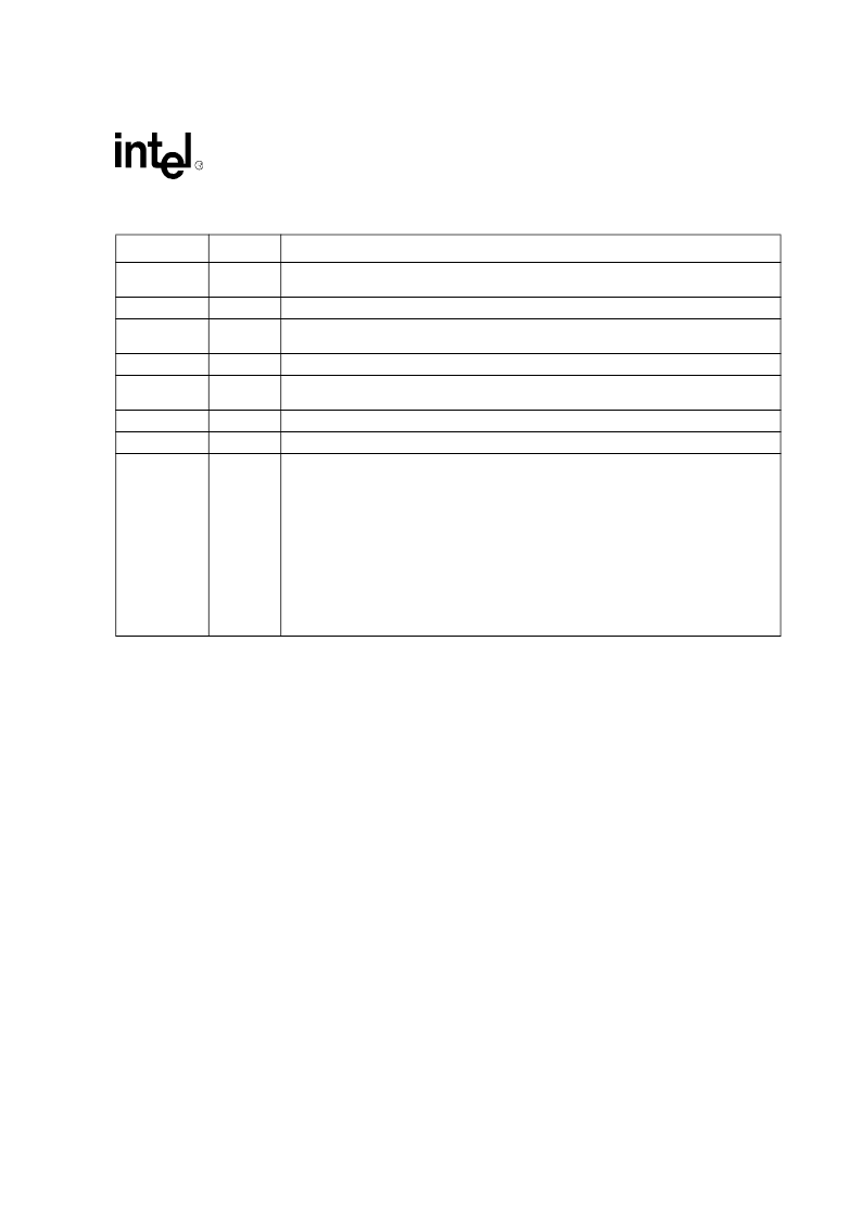
CTS*[0
–
3]
I
CLEAR TO SEND* [0
–
3]:
This input can be programmed to control the flow of transmit data, for
out-of-band flow control applications.
TXCIN
I
TRANSMIT CLOCK:
This pin inputs the transmit clock to the bit rate generator.
CD*
I
CARRIER DETECT*
: This pin is always visible in the MSVR register. CD* is a general purpose
modem input and can be used to cause modem group interrupts upon signal level transitions.
RXCIN
I
RECEIVE CLOCK:
This pin inputs the receive clock to the bit rate generator.
DSR*
I
DATA SET READY*
: This pin is always visible in the MSVR register. DSR* can be used to
validate receive data as well as cause modem group interrupts upon signal level transitions.
TXD[0
–
3]
O
TRANSMIT DATA [0
–
3]:
Serial data output for each channel.
RXD[0
–
3]
I
RECEIVE DATA [0
–
3]:
Serial data input for each channel.
BYTESWAP
I
BYTESWAP:
This pin alters the byte ordering of data during certain 16-bit transfers. It also
changes that half of the data bus on which byte transfers are made, to comply with Intel
or
Motorola
processor systems. BYTESWAP does not alter the bus handshake signals. When
the BYTESWAP pin is high, the byte on A/D[0
–
7] precedes that on A/D[8
–
15] in a string of
transmit or receive bytes. When BYTESWAP is low, A/D[8
–
15] precedes A/D[0
–
7]. When the
BYTESWAP pin is high, bytes are transferred on A/D[0
–
7] when A[0] is low, and on A/D[8
–
15]
when A[0] is high. When BYTESWAP is low, bytes are transferred on A/D[8
–
15] when A[0] is
low, and A/D[0
–
7] when A[0] is high. A different register map is used, depending on the state of
this pin.
Byteswap Byte Alignment
0
Motorola byte alignment
1
Intel byte alignment
Table 1. Pin Descriptions
(Sheet 3 of 3)
Symbol
Type
Description
相關(guān)PDF資料 |
PDF描述 |
|---|---|
| CD3086 | General Purpose NPN Transistor Array |
| CD4000 | CMOS NOR Gates |
| CD4001 | CMOS NOR Gates |
| CD4002 | CMOS NOR Gates |
| CD40011 | Quad 2-Input NOR,NAND Buffered B Series Gate |
相關(guān)代理商/技術(shù)參數(shù) |
參數(shù)描述 |
|---|---|
| CD24B3 031573 | 制造商:Comair Rotron 功能描述:FAN 254MM 24VDC |
| CD24B3 | 制造商:Comair Rotron 功能描述:FAN 254MM 24VDC |
| CD-250 | 制造商:Stellar Labs 功能描述:CD / USB Media Player with FM Tuner - MP3 and WMA |
| CD2500R1 | 制造商:LOGETR 功能描述: |
| CD250-3KVM.25 | 制造商:Yageo / Phycomp 功能描述:CD250-3KVM.25 |
發(fā)布緊急采購,3分鐘左右您將得到回復(fù)。