- 您現(xiàn)在的位置:買賣IC網(wǎng) > PDF目錄379876 > celeron 700 (Intel Corp.) Intel Celeron Processor Up To 700 MHz(頻率達(dá)700MHz的INTEL Celeron 處理器) PDF資料下載
參數(shù)資料
| 型號(hào): | celeron 700 |
| 廠商: | Intel Corp. |
| 英文描述: | Intel Celeron Processor Up To 700 MHz(頻率達(dá)700MHz的INTEL Celeron 處理器) |
| 中文描述: | 英特爾賽揚(yáng)處理器高達(dá)700兆赫(頻率達(dá)700MHz的英特爾賽揚(yáng)處理器的) |
| 文件頁(yè)數(shù): | 47/118頁(yè) |
| 文件大?。?/td> | 990K |
| 代理商: | CELERON 700 |
第1頁(yè)第2頁(yè)第3頁(yè)第4頁(yè)第5頁(yè)第6頁(yè)第7頁(yè)第8頁(yè)第9頁(yè)第10頁(yè)第11頁(yè)第12頁(yè)第13頁(yè)第14頁(yè)第15頁(yè)第16頁(yè)第17頁(yè)第18頁(yè)第19頁(yè)第20頁(yè)第21頁(yè)第22頁(yè)第23頁(yè)第24頁(yè)第25頁(yè)第26頁(yè)第27頁(yè)第28頁(yè)第29頁(yè)第30頁(yè)第31頁(yè)第32頁(yè)第33頁(yè)第34頁(yè)第35頁(yè)第36頁(yè)第37頁(yè)第38頁(yè)第39頁(yè)第40頁(yè)第41頁(yè)第42頁(yè)第43頁(yè)第44頁(yè)第45頁(yè)第46頁(yè)當(dāng)前第47頁(yè)第48頁(yè)第49頁(yè)第50頁(yè)第51頁(yè)第52頁(yè)第53頁(yè)第54頁(yè)第55頁(yè)第56頁(yè)第57頁(yè)第58頁(yè)第59頁(yè)第60頁(yè)第61頁(yè)第62頁(yè)第63頁(yè)第64頁(yè)第65頁(yè)第66頁(yè)第67頁(yè)第68頁(yè)第69頁(yè)第70頁(yè)第71頁(yè)第72頁(yè)第73頁(yè)第74頁(yè)第75頁(yè)第76頁(yè)第77頁(yè)第78頁(yè)第79頁(yè)第80頁(yè)第81頁(yè)第82頁(yè)第83頁(yè)第84頁(yè)第85頁(yè)第86頁(yè)第87頁(yè)第88頁(yè)第89頁(yè)第90頁(yè)第91頁(yè)第92頁(yè)第93頁(yè)第94頁(yè)第95頁(yè)第96頁(yè)第97頁(yè)第98頁(yè)第99頁(yè)第100頁(yè)第101頁(yè)第102頁(yè)第103頁(yè)第104頁(yè)第105頁(yè)第106頁(yè)第107頁(yè)第108頁(yè)第109頁(yè)第110頁(yè)第111頁(yè)第112頁(yè)第113頁(yè)第114頁(yè)第115頁(yè)第116頁(yè)第117頁(yè)第118頁(yè)
Datasheet
47
Intel
Celeron Processor up to 700 MHz
3.2
AGTL+ Signal Quality Specifications and Measurement
Guidelines
Many scenarios have been simulated to generate a set of AGTL+ layout guidelines which are
available in AP-585,
Pentium
II Processor AGTL+ Guidelines
(Order Number 243330). Refer to
the
Pentium
II Processor Developer’s Manual
(Order Number 243502) for the AGTL+ buffer
specification.
Table 27
provides the AGTL+ signal quality specifications (for both the S.E.P. and PPGA
Packages) for use in simulating signal quality at the processor core.
Table 28
provides the AGTL+
signal quality specifications (for the FC-PGA Packages) for use in simulating signal quality at the
processor core.
Table 29
provides AGTL+ signal quality guidelines for measuring and testing
signal quality at the processor edge fingers.
Figure 13
describes the signal quality waveform for
AGTL+ signals at the processor core and edge fingers. For more information on the AGTL+
interface, see the
Pentium
II Processor Developer’s Manual
(Order Number 243502).
NOTES:
1. Unless otherwise noted, all specifications in this table apply to all Intel
Celeron processor frequencies.
2. Specifications are for the edge rate of 0.3 - 0.8 V/ns. See
Figure 13
for the generic waveform.
3. All values specified by design characterization.
4. This specification applies to Intel Celeron processors operating with a 66 MHz Intel Celeron processor
system bus only.
5. Ringback below V
REF
+ 20 mV is not supported.
NOTES:
1. Unless otherwise noted, all specifications in this table apply to all Intel
Celeron
processor frequencies.
2. Specifications are for the edge rate of 0.3 - 0.8V/ns. See
Figure 13
for the generic waveform.
3. All values specified by design characterization.
4. See
Table 32
for maximum allowable overshoot.
5. Ringback between V
REF
+ 100 mV and V
REF
+ 200 mV or V
REF
- 200 mV and V
REF
- 100 mVs requires the
flight time measurements to be adjusted as described in the Intel AGTL+ Specifications (
Intel
Pentium
II
Developers Manual). Ringback below V
REF
+ 100 mV or above V
REF
- 100 mV is not supported.
6. Intel recommends simulations not exceed a ringback value of V
REF
±200 mV to allow margin for other
sources of system noise.
7. A negative value for
ρ
indicates that the amplitude of ringback is above V
REF
. (i.e.,
φ
= -100 mV specifies the
signal cannot ringback below V
REF
+ 100 mV).
8.
φ
and
ρ
: are measured relative to V
REF
.
α
: is measured relative to V
REF
+ 200 mV.
9. All Ringback entering the Overdrive Region must have flight time correction.
10.Overshoot specifications for Ringback do not correspond to Overshoot specifications in
Section 3.4
.
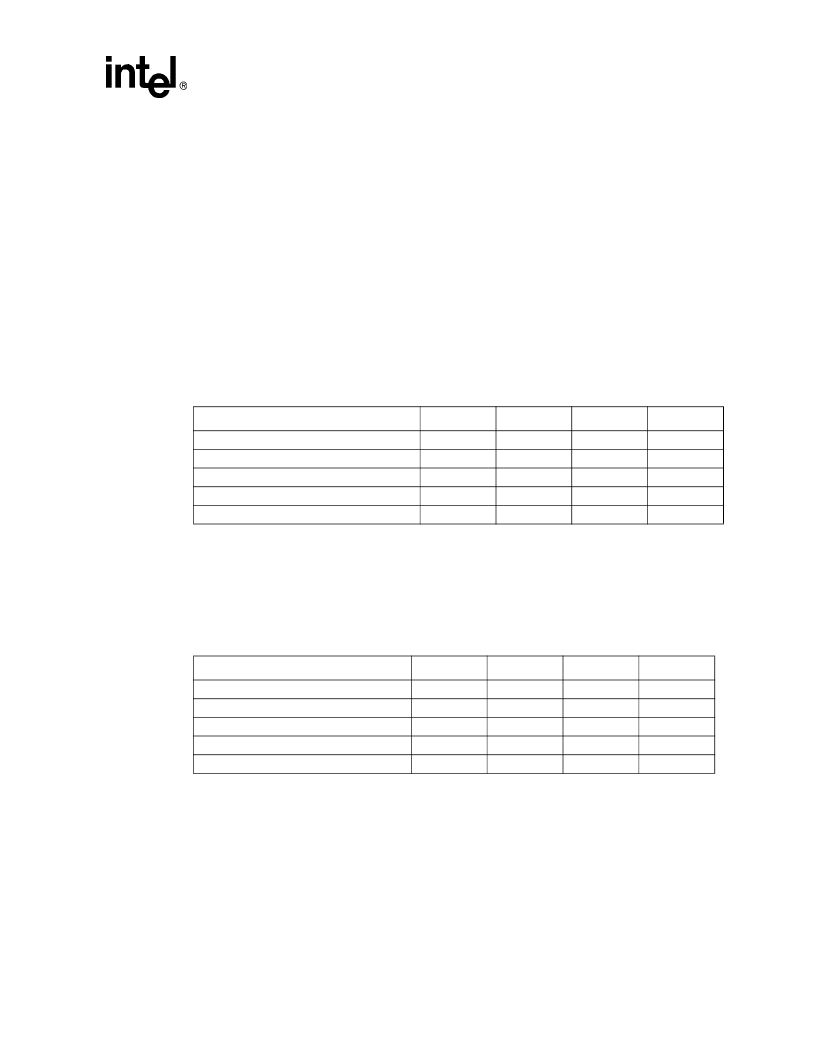
Table 27. AGTL+ Signal Groups Ringback Tolerance Specifications at the Processor Core
(For Both the S.E.P. and PPGA Packages)
1, 2, 3
T# Parameter
Min
Unit
Figure
Notes
α
: Overshoot
τ
: Minimum Time at High
ρ
: Amplitude of Ringback
φ
: Final Settling Voltage
δ
: Duration of Squarewave Ringback
100
mV
13
4
1.00
ns
13
4
–100
mV
13
4, 5
100
mV
13
4
N/A
ns
13
Table 28. AGTL+ Signal Groups Ringback Tolerance Specifications at the Processor Pins
(For FC-PGA Packages)
1, 2, 3
T# Parameter
Min
Unit
Figure
Notes
α
: Overshoot
τ
: Minimum Time at High
ρ
: Amplitude of Ringback
φ
: Final Settling Voltage
δ
: Duration of Squarewave Ringback
100
mV
13
4, 8, 9, 10
0.50
ns
13
9
–200
mV
13
5, 6, 7, 8
200
mV
13
8
N/A
ns
13
相關(guān)PDF資料 |
PDF描述 |
|---|---|
| celeron cpu Mobile Module | processor Mobile Module Connector 1 (MMC-1) at 466 MHz and 433MHZ(工作頻率466和433兆赫茲帶連接器1處理器) |
| celeron CPU with Mobile Module | processor Mobile Module Connector 2 (MMC-2) at 466 MHz and 433MHZ(工作頻率466和433兆赫茲帶連接器2處理器) |
| Celeron Processor with mobile | Celeron Processor Mobile Module MMC-1 at 400 MHz, 366 MHz, 333 MHz, and 300 MHz(工作頻率400,366,333,300和266兆赫茲帶移動(dòng)模塊和連接器1處理器) |
| celeron processor | 32 bit Celeron Processor Mobile Module(32 位帶移動(dòng)模塊處理器) |
| CEM11C2 | Dual Enhancement Mode Field Effect Transistor (N and P Channel) |
相關(guān)代理商/技術(shù)參數(shù) |
參數(shù)描述 |
|---|---|
| CELF001001J1 | 制造商:Panasonic Industrial Company 功能描述:FILTER |
| CELHK11-1REC5-59-3.00-AV-01-V | 功能描述:CIRCUIT BRKR MAG-HYDR LEVER 3A 制造商:sensata technologies/airpax 系列:CEL 零件狀態(tài):有效 斷路器類型:磁性(液力延遲) 額定電流:3A 額定電壓 - AC:- 額定電壓 - DC:- 極數(shù):2 致動(dòng)器類型:搖臂 照明:- 照明電壓(標(biāo)稱值):- 安裝類型:面板安裝 標(biāo)準(zhǔn)包裝:1 |
| CELHK11-1REC5-59-35.0-AV-01-V | 功能描述:CIRCUIT BRKR MAG-HYDR LEVER 35A 制造商:sensata technologies/airpax 系列:CEL 零件狀態(tài):有效 斷路器類型:磁性(液力延遲) 額定電流:35A 額定電壓 - AC:- 額定電壓 - DC:- 極數(shù):2 致動(dòng)器類型:搖臂 照明:- 照明電壓(標(biāo)稱值):- 安裝類型:面板安裝 標(biāo)準(zhǔn)包裝:1 |
| CELHK11-1REC5-71165-10-V | 功能描述:CIRCUIT BREAKER MAG-HYDR LEVER 制造商:sensata technologies/airpax 系列:* 零件狀態(tài):有效 標(biāo)準(zhǔn)包裝:1 |
| CELHK11-1REC5-71165-11-V | 功能描述:CIRCUIT BREAKER MAG-HYDR LEVER 制造商:sensata technologies/airpax 系列:* 零件狀態(tài):有效 標(biāo)準(zhǔn)包裝:1 |
發(fā)布緊急采購(gòu),3分鐘左右您將得到回復(fù)。