- 您現(xiàn)在的位置:買賣IC網(wǎng) > PDF目錄98069 > S1C88848D0A0100 8-BIT, MROM, 8.2 MHz, MICROCONTROLLER, UUC192 PDF資料下載
參數(shù)資料
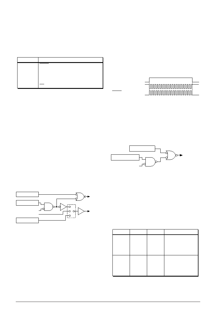
| 型號: | S1C88848D0A0100 |
| 元件分類: | 微控制器/微處理器 |
| 英文描述: | 8-BIT, MROM, 8.2 MHz, MICROCONTROLLER, UUC192 |
| 封裝: | DIE-192 |
| 文件頁數(shù): | 114/174頁 |
| 文件大小: | 1304K |
| 代理商: | S1C88848D0A0100 |
第1頁第2頁第3頁第4頁第5頁第6頁第7頁第8頁第9頁第10頁第11頁第12頁第13頁第14頁第15頁第16頁第17頁第18頁第19頁第20頁第21頁第22頁第23頁第24頁第25頁第26頁第27頁第28頁第29頁第30頁第31頁第32頁第33頁第34頁第35頁第36頁第37頁第38頁第39頁第40頁第41頁第42頁第43頁第44頁第45頁第46頁第47頁第48頁第49頁第50頁第51頁第52頁第53頁第54頁第55頁第56頁第57頁第58頁第59頁第60頁第61頁第62頁第63頁第64頁第65頁第66頁第67頁第68頁第69頁第70頁第71頁第72頁第73頁第74頁第75頁第76頁第77頁第78頁第79頁第80頁第81頁第82頁第83頁第84頁第85頁第86頁第87頁第88頁第89頁第90頁第91頁第92頁第93頁第94頁第95頁第96頁第97頁第98頁第99頁第100頁第101頁第102頁第103頁第104頁第105頁第106頁第107頁第108頁第109頁第110頁第111頁第112頁第113頁當前第114頁第115頁第116頁第117頁第118頁第119頁第120頁第121頁第122頁第123頁第124頁第125頁第126頁第127頁第128頁第129頁第130頁第131頁第132頁第133頁第134頁第135頁第136頁第137頁第138頁第139頁第140頁第141頁第142頁第143頁第144頁第145頁第146頁第147頁第148頁第149頁第150頁第151頁第152頁第153頁第154頁第155頁第156頁第157頁第158頁第159頁第160頁第161頁第162頁第163頁第164頁第165頁第166頁第167頁第168頁第169頁第170頁第171頁第172頁第173頁第174頁
36
EPSON
S1C88848 TECHNICAL MANUAL
5 PERIPHERAL CIRCUITS AND THEIR OPERATION (Output Ports)
5.5.5 Special output
Besides normal DC output, each output port can
also be assigned special output function by
software (R27, R34, R50) or mask option (R26, R51)
as shown in Table 5.5.5.1.
Table 5.5.5.1 Special output ports
Output port
R26
R27
R34
R50
R51
Special output
TOUT output or REM output (mask option)
TOUT output (software selection)
FOUT output (software selection)
BZ output (software selection)
BZ output (mask option)
■ REM output (R26)
A mask option is provided so the R26 output port
terminal can be used for outputting a REM signal
(remote control carrier signal).
When REM output is selected, the R26 data register
is disconnected from the R26 terminal and can be
used as a general-purpose register that does not
affect the output.
The REM output is controlled using the remote
controller registers. Refer to Section 5.13, "Remote
Controller" for details.
■
_________
TOUT output (R27), TOUT output (R26)
In order for the S1C88848 to provide clock signal to
an external device, the R27 output port terminal can
be used to output a TOUT signal (clock output by
the programmable timer). Furthermore, the R26
_________
output port terminal can be used to output a TOUT
signal (TOUT inverted signal). The configuration of
the output ports R26 and R27 is shown in Figure
5.5.5.1.
Register R27D
Register PTOUT
R27 output
R26 output
Mask option
TOUT signal
REM signal
Register R26D
Fig. 5.5.5.1 Configuration of R26 and R27
_________
The output control for the TOUT (TOUT) signals is
done by the register PTOUT. When you set "1" for
_________
the PTOUT, the TOUT (TOUT) signal is output
from the R27 (R26) output port terminal. When "0"
is set, the R27 goes HIGH (VDD) and the R26 goes
LOW (VSS).
To output the TOUT signal, "1" must always be set
for the data register R27D.
_________
The data register R26D does not affect the TOUT
output.
The TOUT signal is generated from the
programmable timer underflow signal by halving
the frequency.
With respect to frequency control, see "5.10 Pro-
grammable Timer".
_________
Since the TOUT (TOUT) signal is generated asyn-
chronously from the register PTOUT, when the
signal is turned ON or OFF by setting the register, a
hazard of a 1/2 cycle or less is generated.
Figure 5.5.5.2 shows the output waveform of the
_________
TOUT (TOUT) signal.
PTOUT
TOUT output (R27)
TOUT output (R26) *
01
when selected by mask option
________
Fig. 5.5.5.2 TOUT (TOUT) output waveform
■ FOUT output (R34)
In order for the S1C88848 to provide clock signal to
an external device, a FOUT signal (divided clock of
oscillation clock fOSC1 or fOSC3) can be output from
the output port terminal R34.
Figure 5.5.5.3 shows the configuration of output
port R34.
Register R34D
Register FOUTON
R34 output
FOUT signal
Fig. 5.5.5.3 Configuration of R34
The output control for the FOUT signal is done by
the register FOUTON. When you set "1" for the
FOUTON, the FOUT signal is output from the
output port terminal R34, when "0" is set, the HIGH
(VDD) level is output. At this time, "1" must always
be set for the data register R34D.
The frequency of the FOUT signal can be selected in
software by setting the registers FOUT0–FOUT2.
The frequency is selected any one from among
eight settings as shown in Table 5.5.5.2.
Table 5.5.5.2 FOUT frequency setting
FOUT2
FOUT frequency
0
1
fOSC1 / 1
fOSC1 / 2
fOSC1 / 4
fOSC1 / 8
fOSC3 / 1
fOSC3 / 2
fOSC3 / 4
fOSC3 / 8
FOUT1
0
1
0
1
FOUT0
0
1
0
1
0
1
0
1
fOSC1:
fOSC3:
OSC1 oscillation frequency
OSC3 oscillation frequency
相關PDF資料 |
PDF描述 |
|---|---|
| S1C8F360F | 8-BIT, FLASH, 8.2 MHz, MICROCONTROLLER, PQFP176 |
| S1D13305F00B | 640 X 256 PIXELS CRT CHAR OR GRPH DSPL CTLR, PQFP60 |
| S1D13305F00A | 640 X 256 PIXELS CRT CHAR OR GRPH DSPL CTLR, PQFP60 |
| S1D13600F00A | CRT OR FLAT PNL GRPH DSPL CTLR, PQFP64 |
| S1D13700F02A100 | 320 X 240 PIXELS CRT OR FLAT PNL GRPH DSPL CTLR, PQFP64 |
相關代理商/技術參數(shù) |
參數(shù)描述 |
|---|---|
| S1C8F360D411000 | 功能描述:16位微控制器 - MCU 8-bit Flash 60KB LCD Dr. 51 x 32 RoHS:否 制造商:Texas Instruments 核心:RISC 處理器系列:MSP430FR572x 數(shù)據(jù)總線寬度:16 bit 最大時鐘頻率:24 MHz 程序存儲器大小:8 KB 數(shù)據(jù) RAM 大小:1 KB 片上 ADC:Yes 工作電源電壓:2 V to 3.6 V 工作溫度范圍:- 40 C to + 85 C 封裝 / 箱體:VQFN-40 安裝風格:SMD/SMT |
| S1C8F360D511000 | 功能描述:16位微控制器 - MCU 8-bit Flash 60KB LCD Dr. 51 x 32 RoHS:否 制造商:Texas Instruments 核心:RISC 處理器系列:MSP430FR572x 數(shù)據(jù)總線寬度:16 bit 最大時鐘頻率:24 MHz 程序存儲器大小:8 KB 數(shù)據(jù) RAM 大小:1 KB 片上 ADC:Yes 工作電源電壓:2 V to 3.6 V 工作溫度范圍:- 40 C to + 85 C 封裝 / 箱體:VQFN-40 安裝風格:SMD/SMT |
| S1C8F360F413100 | 功能描述:16位微控制器 - MCU 8-bit Flash 60KB LCD Dr. 51 x 32 RoHS:否 制造商:Texas Instruments 核心:RISC 處理器系列:MSP430FR572x 數(shù)據(jù)總線寬度:16 bit 最大時鐘頻率:24 MHz 程序存儲器大小:8 KB 數(shù)據(jù) RAM 大小:1 KB 片上 ADC:Yes 工作電源電壓:2 V to 3.6 V 工作溫度范圍:- 40 C to + 85 C 封裝 / 箱體:VQFN-40 安裝風格:SMD/SMT |
| S1C8F360F513200 | 功能描述:16位微控制器 - MCU 8-bit Flash 60KB LCD Dr. 51 x 32 RoHS:否 制造商:Texas Instruments 核心:RISC 處理器系列:MSP430FR572x 數(shù)據(jù)總線寬度:16 bit 最大時鐘頻率:24 MHz 程序存儲器大小:8 KB 數(shù)據(jù) RAM 大小:1 KB 片上 ADC:Yes 工作電源電壓:2 V to 3.6 V 工作溫度范圍:- 40 C to + 85 C 封裝 / 箱體:VQFN-40 安裝風格:SMD/SMT |
| S1C8F626 | 制造商:EPSON 制造商全稱:EPSON 功能描述:8-bit Single Chip Microcomputer |
發(fā)布緊急采購,3分鐘左右您將得到回復。