- 您現(xiàn)在的位置:買(mǎi)賣(mài)IC網(wǎng) > PDF目錄1977 > XRT94L31IB-L (Exar Corporation)IC MAPPER DS3/E3/STS-1 504TBGA PDF資料下載
參數(shù)資料
| 型號(hào): | XRT94L31IB-L |
| 廠(chǎng)商: | Exar Corporation |
| 文件頁(yè)數(shù): | 26/133頁(yè) |
| 文件大?。?/td> | 0K |
| 描述: | IC MAPPER DS3/E3/STS-1 504TBGA |
| 標(biāo)準(zhǔn)包裝: | 24 |
| 應(yīng)用: | 網(wǎng)絡(luò)切換 |
| 接口: | 總線(xiàn) |
| 電源電壓: | 3.14 V ~ 3.47 V |
| 封裝/外殼: | 504-LBGA |
| 供應(yīng)商設(shè)備封裝: | 504-TBGA(35x35) |
| 包裝: | 托盤(pán) |
| 安裝類(lèi)型: | 表面貼裝 |
第1頁(yè)第2頁(yè)第3頁(yè)第4頁(yè)第5頁(yè)第6頁(yè)第7頁(yè)第8頁(yè)第9頁(yè)第10頁(yè)第11頁(yè)第12頁(yè)第13頁(yè)第14頁(yè)第15頁(yè)第16頁(yè)第17頁(yè)第18頁(yè)第19頁(yè)第20頁(yè)第21頁(yè)第22頁(yè)第23頁(yè)第24頁(yè)第25頁(yè)當(dāng)前第26頁(yè)第27頁(yè)第28頁(yè)第29頁(yè)第30頁(yè)第31頁(yè)第32頁(yè)第33頁(yè)第34頁(yè)第35頁(yè)第36頁(yè)第37頁(yè)第38頁(yè)第39頁(yè)第40頁(yè)第41頁(yè)第42頁(yè)第43頁(yè)第44頁(yè)第45頁(yè)第46頁(yè)第47頁(yè)第48頁(yè)第49頁(yè)第50頁(yè)第51頁(yè)第52頁(yè)第53頁(yè)第54頁(yè)第55頁(yè)第56頁(yè)第57頁(yè)第58頁(yè)第59頁(yè)第60頁(yè)第61頁(yè)第62頁(yè)第63頁(yè)第64頁(yè)第65頁(yè)第66頁(yè)第67頁(yè)第68頁(yè)第69頁(yè)第70頁(yè)第71頁(yè)第72頁(yè)第73頁(yè)第74頁(yè)第75頁(yè)第76頁(yè)第77頁(yè)第78頁(yè)第79頁(yè)第80頁(yè)第81頁(yè)第82頁(yè)第83頁(yè)第84頁(yè)第85頁(yè)第86頁(yè)第87頁(yè)第88頁(yè)第89頁(yè)第90頁(yè)第91頁(yè)第92頁(yè)第93頁(yè)第94頁(yè)第95頁(yè)第96頁(yè)第97頁(yè)第98頁(yè)第99頁(yè)第100頁(yè)第101頁(yè)第102頁(yè)第103頁(yè)第104頁(yè)第105頁(yè)第106頁(yè)第107頁(yè)第108頁(yè)第109頁(yè)第110頁(yè)第111頁(yè)第112頁(yè)第113頁(yè)第114頁(yè)第115頁(yè)第116頁(yè)第117頁(yè)第118頁(yè)第119頁(yè)第120頁(yè)第121頁(yè)第122頁(yè)第123頁(yè)第124頁(yè)第125頁(yè)第126頁(yè)第127頁(yè)第128頁(yè)第129頁(yè)第130頁(yè)第131頁(yè)第132頁(yè)第133頁(yè)
XRT94L31
121
REV. 1.0.1
3-CHANNEL DS3/E3/STS-1 TO STS-3/STM-1 MAPPER IC
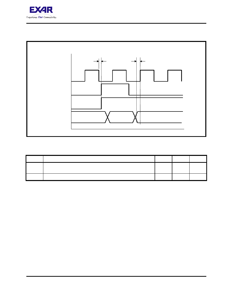
NOTE: The values for t21 and t22 can be found in
1.8
TRANSMIT SECTION DCC INSERTION INPUT PORT
The Transmit Section DCC Insertion Input Port provides a dedicated port for the user to insert his/her own
value for the D1, D2 and D3 bytes within the outbound STS-3/STM-1 data-stream. The user should note that
the TxSDCC input pin is sampled (by the Transmit Section DCC Insertion Input Port) upon the rising edge of
TxTOHClk. The TxSDCCEnable output signal is updated upon the falling edge of TxTOHClk. The timing
wave-form and information for the Transmit Section DCC Insertion Input Port is presented below.
FIGURE 24. ILLUSTRATION OF THE TIMING WAVE-FORM OF THE TRANSMIT ORDER-WIRE BYTE OVERHEAD INPUT
PORT
TABLE 25: TIMING INFORMATION FOR THE TRANSMIT ORDER-WIRE BYTE OVERHEAD INPUT PORT
SYMBOL
DESCRIPTION
MIN.
TYP.
MAX.
t21
Falling edge of TxTOHClk to rising edge of TxE1F1F2Enable and
TxE1F1F2Frame
-0.5ns
0ns
t22
TxE1F1F2 Data to rising edge of TxTOHClk set-up time
4ns
TxE1F1E2
TxTOHClk
TxE1F1E2Fr
TxE1F1E2Enb
t21
t22
相關(guān)PDF資料 |
PDF描述 |
|---|---|
| XRT94L33IB-L | IC MAPPER DS3/E3/STS-1 504TBGA |
| XRT94L43IB-F | IC MAPPER SONET/SDH OC12 516BGA |
| XS1-G02B-FB144-I4 | IC MCU 32BIT 16KB OTP 144FBGA |
| XTR114U/2K5 | IC 4-20MA I-TRANSMITTER 14-SOIC |
| ZXHF5000JB24TC | IC SWITCH QUAD 2X1 24QFN |
相關(guān)代理商/技術(shù)參數(shù) |
參數(shù)描述 |
|---|---|
| XRT94L33 | 制造商:EXAR 制造商全稱(chēng):EXAR 功能描述:-CHANNEL DS3/E3/STS-1 TO STS-3/STM-1 MAPPER - SONET REGISTERS |
| XRT94L33_06 | 制造商:EXAR 制造商全稱(chēng):EXAR 功能描述:3-CHANNEL DS3/E3/STS-1 TO STS-3/STM-1 MAPPER IC DATA SHEET |
| XRT94L33_07 | 制造商:EXAR 制造商全稱(chēng):EXAR 功能描述:3-CHANNEL DS3/E3/STS-1 TO STS-3/STM-1 MAPPER - ATM REGISTERS |
| XRT94L33_1 | 制造商:EXAR 制造商全稱(chēng):EXAR 功能描述:3-CHANNEL DS3/E3/STS-1 TO STS-3/STM-1 MAPPER ATM/PPP - HARWARE MANUAL |
| XRT94L33_2 | 制造商:EXAR 制造商全稱(chēng):EXAR 功能描述:3-CHANNEL DS3/E3/STS-1 TO STS-3/STM-1 MAPPER - SDH REGISTERS |
發(fā)布緊急采購(gòu),3分鐘左右您將得到回復(fù)。