- 您現(xiàn)在的位置:買賣IC網(wǎng) > PDF目錄98081 > SIO10N268-NU (STANDARD MICROSYSTEMS CORP) MULTIFUNCTION PERIPHERAL, PQFP128 PDF資料下載
參數(shù)資料
| 型號: | SIO10N268-NU |
| 廠商: | STANDARD MICROSYSTEMS CORP |
| 元件分類: | 外設(shè)及接口 |
| 英文描述: | MULTIFUNCTION PERIPHERAL, PQFP128 |
| 封裝: | 14 X 14 MM, 1MM THICKNESS, GREEN, TQFP-128 |
| 文件頁數(shù): | 191/251頁 |
| 文件大?。?/td> | 1384K |
| 代理商: | SIO10N268-NU |
第1頁第2頁第3頁第4頁第5頁第6頁第7頁第8頁第9頁第10頁第11頁第12頁第13頁第14頁第15頁第16頁第17頁第18頁第19頁第20頁第21頁第22頁第23頁第24頁第25頁第26頁第27頁第28頁第29頁第30頁第31頁第32頁第33頁第34頁第35頁第36頁第37頁第38頁第39頁第40頁第41頁第42頁第43頁第44頁第45頁第46頁第47頁第48頁第49頁第50頁第51頁第52頁第53頁第54頁第55頁第56頁第57頁第58頁第59頁第60頁第61頁第62頁第63頁第64頁第65頁第66頁第67頁第68頁第69頁第70頁第71頁第72頁第73頁第74頁第75頁第76頁第77頁第78頁第79頁第80頁第81頁第82頁第83頁第84頁第85頁第86頁第87頁第88頁第89頁第90頁第91頁第92頁第93頁第94頁第95頁第96頁第97頁第98頁第99頁第100頁第101頁第102頁第103頁第104頁第105頁第106頁第107頁第108頁第109頁第110頁第111頁第112頁第113頁第114頁第115頁第116頁第117頁第118頁第119頁第120頁第121頁第122頁第123頁第124頁第125頁第126頁第127頁第128頁第129頁第130頁第131頁第132頁第133頁第134頁第135頁第136頁第137頁第138頁第139頁第140頁第141頁第142頁第143頁第144頁第145頁第146頁第147頁第148頁第149頁第150頁第151頁第152頁第153頁第154頁第155頁第156頁第157頁第158頁第159頁第160頁第161頁第162頁第163頁第164頁第165頁第166頁第167頁第168頁第169頁第170頁第171頁第172頁第173頁第174頁第175頁第176頁第177頁第178頁第179頁第180頁第181頁第182頁第183頁第184頁第185頁第186頁第187頁第188頁第189頁第190頁當前第191頁第192頁第193頁第194頁第195頁第196頁第197頁第198頁第199頁第200頁第201頁第202頁第203頁第204頁第205頁第206頁第207頁第208頁第209頁第210頁第211頁第212頁第213頁第214頁第215頁第216頁第217頁第218頁第219頁第220頁第221頁第222頁第223頁第224頁第225頁第226頁第227頁第228頁第229頁第230頁第231頁第232頁第233頁第234頁第235頁第236頁第237頁第238頁第239頁第240頁第241頁第242頁第243頁第244頁第245頁第246頁第247頁第248頁第249頁第250頁第251頁
Advanced Notebook I/O for ISA or LPC Designs
Datasheet
Rev. 0.5 (03-24-05)
Page 44
SMSC SIO10N268
DATASHEET
clocks 1 and 2 of the SYNC phase and ‘0000b’ for the last clock of the SYNC phase. This would be
equivalent to 5 clocks worth of access time if the device started that access at the conclusion of the
MADDR phase. Once SYNC is achieved, the device returns the data in two clocks and gives ownership of
the bus back to the host with a TAR phase.
8.4.7
Write Cycles
8.4.7.1
Single Byte
All devices that support FWH Memory Write cycles must support single byte writes. FWH Memory Write
cycles use the same preamble as FWH Memory read cycles.
To indicate that a single byte transfer cycle is being performed, the master asserts an MSIZE value of 0.
After the address and size has been transferred, the 2-clock data phase begins. Following the data phase,
bus ownership is transferred to the FWH component with a TAR cycle. Following the TAR phase, the
device must assert a SYNC value of ‘0000b’ (ready) or ‘1010b’ (error) indicating the data has been
received. Bus ownership is then given back to the master with another TAR phase.
FWH Memory Writes only allow one clock for the SYNC phase. The TAR+SYNC+TAR phases at the end
of FWH memory write cycles must be exactly 5 clocks.
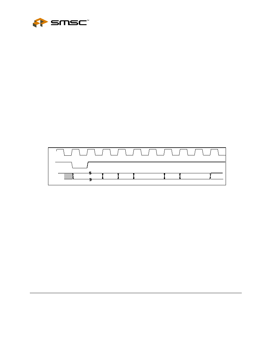
Preamble
D L
SYNC
CLK
FRAME#
TAR
AD[3:0]
10 Clocks
D H
TAR
Figure 8.3 - Single Byte Write
8.4.8
Error Reporting
There is no error reporting over the FWH interface for FWH Memory cycles. If an error occurs, such as an
address out of range or an unsupported memory size, the cycle will continue from the host unabated. This
is because these errors are the result of illegal programming, and there is no efficient error reporting
method that can be done to counter the programming error.
Therefore, the FWH component must not report the error conditions over the FWH interface. It must only
report wait states and the ‘ready’ condition. It may choose to log the error internally to be debugged, but it
must not signal an error through the FWH interface itself.
8.4.9
FWH Cycle Examples
8.4.9.1
EXAMPLE 1: FWH 1-Byte Read
FIELD
DRIVEN BY
CLOCKS
LAD[3:0]
COMMENT
START
Host
1
1101
LAD[3:0]=1101 (FWH Memory Read)
IDSEL
Host
1
xxxx
LAD[3:0]=selected FWH component
MADDR
Host
1
xxxx
Most significant nibble
相關(guān)PDF資料 |
PDF描述 |
|---|---|
| SIS300 | GRAPHICS PROCESSOR, PBGA365 |
| SK12430PJT | 800 MHz, OTHER CLOCK GENERATOR, PQCC28 |
| SK12439PJ | 800 MHz, OTHER CLOCK GENERATOR, PQCC28 |
| SK12439PJT | 800 MHz, OTHER CLOCK GENERATOR, PQCC28 |
| SL15100ZIT-XXX | 200 MHz, OTHER CLOCK GENERATOR, PDSO8 |
相關(guān)代理商/技術(shù)參數(shù) |
參數(shù)描述 |
|---|---|
| SIO665GT | 功能描述:界面開發(fā)工具 Evaluation Board RoHS:否 制造商:Bourns 產(chǎn)品:Evaluation Boards 類型:RS-485 工具用于評估:ADM3485E 接口類型:RS-485 工作電源電壓:3.3 V |
| SIO666GT | 功能描述:界面開發(fā)工具 Evaluation Board RoHS:否 制造商:Bourns 產(chǎn)品:Evaluation Boards 類型:RS-485 工具用于評估:ADM3485E 接口類型:RS-485 工作電源電壓:3.3 V |
| SIO669 | 功能描述:界面開發(fā)工具 Evaluation Board RoHS:否 制造商:Bourns 產(chǎn)品:Evaluation Boards 類型:RS-485 工具用于評估:ADM3485E 接口類型:RS-485 工作電源電壓:3.3 V |
| SIOLS1000V2 | 制造商:SECELECTRONICS 制造商全稱:SECELECTRONICS 功能描述:Current Sensors |
| SIOLS2000V2 | 制造商:SECELECTRONICS 制造商全稱:SECELECTRONICS 功能描述:Current Sensors |
發(fā)布緊急采購,3分鐘左右您將得到回復。