- 您現(xiàn)在的位置:買賣IC網(wǎng) > PDF目錄98068 > S1C88104P0A0100 8-BIT, MROM, 8.2 MHz, MICROCONTROLLER, PBGA240 PDF資料下載
參數(shù)資料
| 型號: | S1C88104P0A0100 |
| 元件分類: | 微控制器/微處理器 |
| 英文描述: | 8-BIT, MROM, 8.2 MHz, MICROCONTROLLER, PBGA240 |
| 封裝: | VFBGA10H-216 |
| 文件頁數(shù): | 156/211頁 |
| 文件大小: | 1802K |
| 代理商: | S1C88104P0A0100 |
第1頁第2頁第3頁第4頁第5頁第6頁第7頁第8頁第9頁第10頁第11頁第12頁第13頁第14頁第15頁第16頁第17頁第18頁第19頁第20頁第21頁第22頁第23頁第24頁第25頁第26頁第27頁第28頁第29頁第30頁第31頁第32頁第33頁第34頁第35頁第36頁第37頁第38頁第39頁第40頁第41頁第42頁第43頁第44頁第45頁第46頁第47頁第48頁第49頁第50頁第51頁第52頁第53頁第54頁第55頁第56頁第57頁第58頁第59頁第60頁第61頁第62頁第63頁第64頁第65頁第66頁第67頁第68頁第69頁第70頁第71頁第72頁第73頁第74頁第75頁第76頁第77頁第78頁第79頁第80頁第81頁第82頁第83頁第84頁第85頁第86頁第87頁第88頁第89頁第90頁第91頁第92頁第93頁第94頁第95頁第96頁第97頁第98頁第99頁第100頁第101頁第102頁第103頁第104頁第105頁第106頁第107頁第108頁第109頁第110頁第111頁第112頁第113頁第114頁第115頁第116頁第117頁第118頁第119頁第120頁第121頁第122頁第123頁第124頁第125頁第126頁第127頁第128頁第129頁第130頁第131頁第132頁第133頁第134頁第135頁第136頁第137頁第138頁第139頁第140頁第141頁第142頁第143頁第144頁第145頁第146頁第147頁第148頁第149頁第150頁第151頁第152頁第153頁第154頁第155頁當(dāng)前第156頁第157頁第158頁第159頁第160頁第161頁第162頁第163頁第164頁第165頁第166頁第167頁第168頁第169頁第170頁第171頁第172頁第173頁第174頁第175頁第176頁第177頁第178頁第179頁第180頁第181頁第182頁第183頁第184頁第185頁第186頁第187頁第188頁第189頁第190頁第191頁第192頁第193頁第194頁第195頁第196頁第197頁第198頁第199頁第200頁第201頁第202頁第203頁第204頁第205頁第206頁第207頁第208頁第209頁第210頁第211頁
S1C8F626 TECHNICAL MANUAL
EPSON
41
5 PERIPHERAL CIRCUITS AND THEIR OPERATION (Input Ports)
K00D–K07D: 00FF54H
Input data of input port terminal K0x can be read
out.
When "1" is read:
HIGH level
When "0" is read:
LOW level
Writing:
Invalid
The terminal voltage of each of the input port K00–
K07 can be directly read out as either a "1" for
HIGH (VDD) level or a "0" for LOW (VSS) level.
This bit is exclusively for readout and are not
usable for write operations.
IFLK00–IFLK07: 00FF5AH
Selects an input interface level.
When "1" is written: CMOS Schmitt level
When "0" is written: CMOS level
Reading:
Valid
IFLK0x is the input I/F level select register
corresponding to each input port K0x.
When "1" is written to IFLK0x, the corresponding
input port K0x is configured with a CMOS Schmitt
level interface. When "0" is written, the port is
configured with a CMOS level interface.
At initial reset, this register is set to "0" (CMOS
level).
PULK00–PULK07: 00FF56H
Controls the input pull-up resistor.
When "1" is written: Pull-up ON
When "0" is written: Pull-up OFF
Reading:
Valid
PULK0x is the pull-up control register
corresponding to the input port K0x that turns the
pull-up resistor built into the input port ON and
OFF.
When "1" is written to PULK0x, the corresponding
input port K0x is pulled up to high. When "0" is
written, the input port is not pulled up.
At initial reset, this register is set to "1" (Pull-up
ON).
KCP00–KCP07: 00FF52H
Sets the interrupt generation condition (interrupt
generation timing) for input port terminals K00–
K07.
When "1" is written: Falling edge
When "0" is written: Rising edge
Reading:
Valid
KCP0x is the input comparison register which
corresponds to the input port K0x. Interrupt in
those ports which have been set to "1" is generated
on the falling edge of the input and in those set to
"0" on the rising edge.
At initial reset, this register is set to "1" (falling
edge).
CTK00L–CTK02L: 00FF58HD0–D2
Sets the input level check time of the chattering-
eliminate circuit for the K00–K03 input port
interrupts as shown in Table 5.5.5.2.
Table 5.5.5.2 Setting the input level check time
CTK02L
1
0
CTK01L
1
0
1
0
CTK00L
1
0
1
0
1
0
1
0
Input level check time [sec]
4/fOSC3
2/fOSC3
1/fOSC3
4096/fOSC1
2048/fOSC1
512/fOSC1
128/fOSC1
None
Be sure to disable interrupts before changing the
contents of this register. Unnecessary interrupts
may occur if the register is changed when the
corresponding input port interrupts have been
enabled by the interrupt enable register EK0x.
At initial reset, this register is set to "0" (None).
CTK00H–CTK02H: 00FF58HD4–D6
Sets the input level check time of the chattering-
eliminate circuit for the K04–K07 input port
interrupts as shown in Table 5.5.5.3.
Table 5.5.5.3 Setting the input level check time
CTK02H
1
0
CTK01H
1
0
1
0
CTK00H
1
0
1
0
1
0
1
0
Input level check time [sec]
4/fOSC3
2/fOSC3
1/fOSC3
4096/fOSC1
2048/fOSC1
512/fOSC1
128/fOSC1
None
Be sure to disable interrupts before changing the
contents of this register. Unnecessary interrupt may
occur if the register is changed when the
corresponding input port interrupts have been
enabled by the interrupt enable register EK0x.
At initial reset, this register is set to "0" (None).
PK00, PK01: 00FF20HD6, D7
Sets the input interrupt priority level. PK00 and
PK01 are the interrupt priority registers
corresponding to the input interrupts.
Table 5.5.5.4 shows the interrupt priority level
which can be set by this register.
Table 5.5.5.4 Interrupt priority level settings
PK01
PK00
Interrupt priority level
1
0
1
0
1
0
Level 3 (IRQ3)
Level 2 (IRQ2)
Level 1 (IRQ1)
Level 0 (None)
At initial reset, this register is set to "0" (level 0).
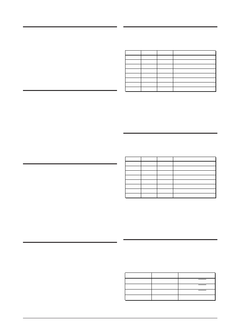
相關(guān)PDF資料 |
PDF描述 |
|---|---|
| S1C88317D0A0100 | MICROCONTROLLER, UUC170 |
| S1C88308D0A0100 | MICROCONTROLLER, UUC170 |
| S1C88308F0A0100 | MICROCONTROLLER, PQFP160 |
| S1C88348F | 8-BIT, MROM, 8.2 MHz, MICROCONTROLLER, PQFP16 |
| S1C88316D | 8-BIT, MROM, 8.2 MHz, MICROCONTROLLER, UUC172 |
相關(guān)代理商/技術(shù)參數(shù) |
參數(shù)描述 |
|---|---|
| S1C88349 | 制造商:EPSON 制造商全稱:EPSON 功能描述:8-bit Single Chip Microcomputer |
| S1C88649 | 制造商:EPSON 制造商全稱:EPSON 功能描述:8-bit Single Chip Microcomputer |
| S1C88650 | 制造商:EPSON 制造商全稱:EPSON 功能描述:8-bit Single Chip Microcomputer |
| S1C88655 | 制造商:EPSON 制造商全稱:EPSON 功能描述:8-bit Single Chip Microcomputer |
| S1C88816 | 制造商:EPSON 制造商全稱:EPSON 功能描述:8-bit Single Chip Microcomputer |
發(fā)布緊急采購,3分鐘左右您將得到回復(fù)。