- 您現(xiàn)在的位置:買賣IC網(wǎng) > PDF目錄1958 > ORT8850L-3BM680C (Lattice Semiconductor Corporation)IC FPSC TRANSCEIVER 8CH 680-BGA PDF資料下載
參數(shù)資料
| 型號: | ORT8850L-3BM680C |
| 廠商: | Lattice Semiconductor Corporation |
| 文件頁數(shù): | 56/105頁 |
| 文件大小: | 0K |
| 描述: | IC FPSC TRANSCEIVER 8CH 680-BGA |
| 產(chǎn)品變化通告: | Product Discontinuation 01/Aug/2011 |
| 標(biāo)準(zhǔn)包裝: | 24 |
| 系列: | * |
第1頁第2頁第3頁第4頁第5頁第6頁第7頁第8頁第9頁第10頁第11頁第12頁第13頁第14頁第15頁第16頁第17頁第18頁第19頁第20頁第21頁第22頁第23頁第24頁第25頁第26頁第27頁第28頁第29頁第30頁第31頁第32頁第33頁第34頁第35頁第36頁第37頁第38頁第39頁第40頁第41頁第42頁第43頁第44頁第45頁第46頁第47頁第48頁第49頁第50頁第51頁第52頁第53頁第54頁第55頁當(dāng)前第56頁第57頁第58頁第59頁第60頁第61頁第62頁第63頁第64頁第65頁第66頁第67頁第68頁第69頁第70頁第71頁第72頁第73頁第74頁第75頁第76頁第77頁第78頁第79頁第80頁第81頁第82頁第83頁第84頁第85頁第86頁第87頁第88頁第89頁第90頁第91頁第92頁第93頁第94頁第95頁第96頁第97頁第98頁第99頁第100頁第101頁第102頁第103頁第104頁第105頁
Lattice Semiconductor
ORCA ORT8850 Data Sheet
54
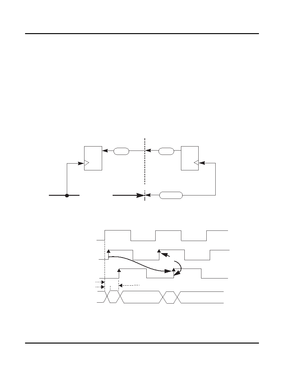
The next two examples show timing for serial TOH data input and output. For these cases, the clock is generated in
the FPGA logic and the discussion accounts for the skew between the clock signal at the FPGA latch and at the
FPGA/Core interface. The clock is routed over a secondary clock path and the skew can vary by ± 3 ns. A value of
+ 2 ns was assumed in the discussions.
Figure 30 shows the timing for sending serial TOH data from the Core to the FPGA logic with data being launched
and latched on the same (rising) clock edge. As in the previous examples, setup and hold time constraints for the
data versus the reference clock at the capturing latch must be met. Data is not captured before the next data is
launched, so there might be a hold time margin problem. Launched data has nearly a full clock period to become
stable at the capture latch and the maximum propagation delay is only 0.2 ns so setup margin should not be a
problem for the timing relationships assumed. Actual timing analysis should be performed for each application
because of the wide range of possible skew values.
Figure 30. Full Cycle, TOH Output Conguration and Timing (-1 Speed Grade)
D
+
Q
+
Δt
Embedded
Core
FPGA
Logic
Secondary Clock
0.4 ns
ASB_TOH_CLK
a. Configuration
b. Timing (ns)
FPGA_CLK
TOH_CLK
±3.0 ns skew
+2.0 ns assumed
TOH_CLK
0.0
4.7
9.4
14.1
18.8
ASB_TOH_CLK
0.4
5.1
8.8
14.5
19.2
Hold
Launch
FPGA_CLK
2.0
6.7
11.4
Capture
16.1
Data Valid
TOH_OUTxx
tprop_max = 2.0
tprop_min = - 0.5
Note: xx - [AA, AB, ..., BD]
TOH_OUTxx
相關(guān)PDF資料 |
PDF描述 |
|---|---|
| P1010PSE5HFA | MPU PROTO 800/667 425-TEPBGA1 |
| P1013NXN2LFB | IC MPU 1067MHZ 689TEPBGA |
| P1013PSE2EFA | IC MPU PROTO 600MHZ 689-TEPBGA |
| P1014NSN5DFA | IC MPU 800MHZ 425TEPBGA1 |
| P1014NSN5FFA | IC MPU 800MHZ 425TEPBGA1 |
相關(guān)代理商/技術(shù)參數(shù) |
參數(shù)描述 |
|---|---|
| ORT8850L-3BMN680C | 功能描述:FPGA - 現(xiàn)場可編程門陣列 4992 LUT 278 I/O RoHS:否 制造商:Altera Corporation 系列:Cyclone V E 柵極數(shù)量: 邏輯塊數(shù)量:943 內(nèi)嵌式塊RAM - EBR:1956 kbit 輸入/輸出端數(shù)量:128 最大工作頻率:800 MHz 工作電源電壓:1.1 V 最大工作溫度:+ 70 C 安裝風(fēng)格:SMD/SMT 封裝 / 箱體:FBGA-256 |
| ORT9303 | 制造商:BOT 制造商全稱:Bedford Opto Technology Ltd. 功能描述:3 ELEMENT PCB MOUNT 1.8mm LED ARRAY |
| ORT9303B | 制造商:BOT 制造商全稱:Bedford Opto Technology Ltd. 功能描述:3 ELEMENT PCB MOUNT 1.8mm LED ARRAY |
| ORT9303BL | 制造商:BOT 制造商全稱:Bedford Opto Technology Ltd. 功能描述:3 ELEMENT PCB MOUNT 1.8mm LED ARRAY |
| ORT9303G | 制造商:BOT 制造商全稱:Bedford Opto Technology Ltd. 功能描述:3 ELEMENT PCB MOUNT 1.8mm LED ARRAY |
發(fā)布緊急采購,3分鐘左右您將得到回復(fù)。