- 您現(xiàn)在的位置:買賣IC網(wǎng) > PDF目錄1958 > ORT8850L-3BM680C (Lattice Semiconductor Corporation)IC FPSC TRANSCEIVER 8CH 680-BGA PDF資料下載
參數(shù)資料
| 型號: | ORT8850L-3BM680C |
| 廠商: | Lattice Semiconductor Corporation |
| 文件頁數(shù): | 52/105頁 |
| 文件大?。?/td> | 0K |
| 描述: | IC FPSC TRANSCEIVER 8CH 680-BGA |
| 產(chǎn)品變化通告: | Product Discontinuation 01/Aug/2011 |
| 標(biāo)準(zhǔn)包裝: | 24 |
| 系列: | * |
第1頁第2頁第3頁第4頁第5頁第6頁第7頁第8頁第9頁第10頁第11頁第12頁第13頁第14頁第15頁第16頁第17頁第18頁第19頁第20頁第21頁第22頁第23頁第24頁第25頁第26頁第27頁第28頁第29頁第30頁第31頁第32頁第33頁第34頁第35頁第36頁第37頁第38頁第39頁第40頁第41頁第42頁第43頁第44頁第45頁第46頁第47頁第48頁第49頁第50頁第51頁當(dāng)前第52頁第53頁第54頁第55頁第56頁第57頁第58頁第59頁第60頁第61頁第62頁第63頁第64頁第65頁第66頁第67頁第68頁第69頁第70頁第71頁第72頁第73頁第74頁第75頁第76頁第77頁第78頁第79頁第80頁第81頁第82頁第83頁第84頁第85頁第86頁第87頁第88頁第89頁第90頁第91頁第92頁第93頁第94頁第95頁第96頁第97頁第98頁第99頁第100頁第101頁第102頁第103頁第104頁第105頁
Lattice Semiconductor
ORCA ORT8850 Data Sheet
50
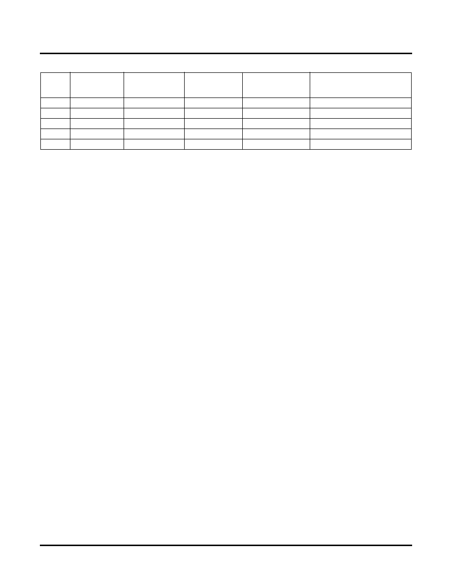
Table 16. Operating Modes and Data Paths - SONET Logic Block
All timing is referenced to the clock signal at the FPGA/Core interface. Data is also timed for signals at the
FPGA/Core interface. There will be additional time delays until the interface signals reach the capturing latch. The
primary or secondary path delay is controlled, as noted earlier, and the clock timing at the capture latch can be pre-
dicted. The data delay, however, may be unique to each interconnect routing.
The timing diagrams provide a quantitative picture of the relative importance of setup and hold margins for the
cases discussed. In the diagrams, the launch and capture times and the time difference between the launching and
capturing clock edges are identied. As the time between launch and capture increases (up to a full clock period),
the possibility of a setup time problem decreases. Also, the possibility of a setup time problem decreases for
smaller maximum propagation delay values.
If capture occurs before the next data is launched, a hold time problem cannot occur. In nearly all cases, the differ-
ence between the launch and capture clock edges will be nearly a full clock cycle and the data will be captured
before the next data is launched. This is not guaranteed, however, and ispLEVER timing analysis should be done
for each application.
The general rules used for the FPGA/Core interface are as follows:
1.
If possible, transfers across the FPGA/Core interface should be direct register to register transfers with minimal
or preferably no intervening logic.
2.
Use positive (rising) edge ip-ops in the FPGA for both input and output unless a timing diagram (case 1)
explicitly indicates otherwise, or a special case (long routing path, etc.) is being considered.
3.
Attempt to ‘locate’ the FPGA side ip-ops reasonably close to the interface unless other timing constraints
prevent this. This ‘locate’ is typically achieved by placing a frequency constraint on the FPGA_CLK signal. In
most cases, up the 3 ns of data path delay through the FPGA logic in the ORT8850 is acceptable.
4.
Pay attention to the clock routing resource recommended (these are xed on the ORT8850), and to the delay
and skew limits and the clock source points.
5.
Run Trace setup and hold checks in ispLEVER on the routed design taking the environmental constraints into
account. (See ispLEVER Application Note for details).
For the cases where parallel data is output from the core, the reference clock is also output from the core and the
effects of propagation delay variation are included in the discussion. Propagation delay is dened relative to the
interface signals and thus is the time from the enabling (falling) edge of the clock from the core to the time that data
is guaranteed to be valid at the interface. As an example, for the rst case discussed, the minimum (tprop_min) and
maximum (tprop_max) propagation delays are 0.8 ns. and 4.7 ns. respectively. Therefore the data outputs are sta-
ble for 6.1 ns. (10 ns. - 3.9 ns.) of each clock cycle. The data must be captured during this stable period, i.e., the
data signals must arrive at the capturing latch with adequate setup and hold margins versus the clock signal at the
latch.
In the rst case, Figure 27, the alignment FIFO is assumed to be bypassed and all timing is with respect to the
recovered clock. The FPGA is latched on the falling edge of the clock, an exception to the general recommenda-
Case
Data (Note: xx
=[AA, …BD])
Data Path
Embedded Core
Clock
Launch/Latch
FPGA Clock
Launch/Latch
Clock/Route
1
DOUTxx[7:0]
Core to FPGA
Falling Edge
CDR_CLK_xx/Secondary
2
DOUTxx[7:0]
Core to FPGA
Falling Edge
Rising Edge
FPGA_SYSCLK/Primary
3
DINxx[7:0]
FPGA to Core
Rising Edge
FPGA_SYSCLK/Primary
4
TOH_OUTxx
Core to FPGA
Rising Edge
From FPGA/Secondary
5
TOH_INxx
FPGA to Core
Falling Edge
Rising Edge
From FPGA/Secondary
相關(guān)PDF資料 |
PDF描述 |
|---|---|
| P1010PSE5HFA | MPU PROTO 800/667 425-TEPBGA1 |
| P1013NXN2LFB | IC MPU 1067MHZ 689TEPBGA |
| P1013PSE2EFA | IC MPU PROTO 600MHZ 689-TEPBGA |
| P1014NSN5DFA | IC MPU 800MHZ 425TEPBGA1 |
| P1014NSN5FFA | IC MPU 800MHZ 425TEPBGA1 |
相關(guān)代理商/技術(shù)參數(shù) |
參數(shù)描述 |
|---|---|
| ORT8850L-3BMN680C | 功能描述:FPGA - 現(xiàn)場可編程門陣列 4992 LUT 278 I/O RoHS:否 制造商:Altera Corporation 系列:Cyclone V E 柵極數(shù)量: 邏輯塊數(shù)量:943 內(nèi)嵌式塊RAM - EBR:1956 kbit 輸入/輸出端數(shù)量:128 最大工作頻率:800 MHz 工作電源電壓:1.1 V 最大工作溫度:+ 70 C 安裝風(fēng)格:SMD/SMT 封裝 / 箱體:FBGA-256 |
| ORT9303 | 制造商:BOT 制造商全稱:Bedford Opto Technology Ltd. 功能描述:3 ELEMENT PCB MOUNT 1.8mm LED ARRAY |
| ORT9303B | 制造商:BOT 制造商全稱:Bedford Opto Technology Ltd. 功能描述:3 ELEMENT PCB MOUNT 1.8mm LED ARRAY |
| ORT9303BL | 制造商:BOT 制造商全稱:Bedford Opto Technology Ltd. 功能描述:3 ELEMENT PCB MOUNT 1.8mm LED ARRAY |
| ORT9303G | 制造商:BOT 制造商全稱:Bedford Opto Technology Ltd. 功能描述:3 ELEMENT PCB MOUNT 1.8mm LED ARRAY |
發(fā)布緊急采購,3分鐘左右您將得到回復(fù)。