- 您現(xiàn)在的位置:買賣IC網(wǎng) > PDF目錄1958 > ORT8850L-3BM680C (Lattice Semiconductor Corporation)IC FPSC TRANSCEIVER 8CH 680-BGA PDF資料下載
參數(shù)資料
| 型號: | ORT8850L-3BM680C |
| 廠商: | Lattice Semiconductor Corporation |
| 文件頁數(shù): | 35/105頁 |
| 文件大?。?/td> | 0K |
| 描述: | IC FPSC TRANSCEIVER 8CH 680-BGA |
| 產(chǎn)品變化通告: | Product Discontinuation 01/Aug/2011 |
| 標準包裝: | 24 |
| 系列: | * |
第1頁第2頁第3頁第4頁第5頁第6頁第7頁第8頁第9頁第10頁第11頁第12頁第13頁第14頁第15頁第16頁第17頁第18頁第19頁第20頁第21頁第22頁第23頁第24頁第25頁第26頁第27頁第28頁第29頁第30頁第31頁第32頁第33頁第34頁當前第35頁第36頁第37頁第38頁第39頁第40頁第41頁第42頁第43頁第44頁第45頁第46頁第47頁第48頁第49頁第50頁第51頁第52頁第53頁第54頁第55頁第56頁第57頁第58頁第59頁第60頁第61頁第62頁第63頁第64頁第65頁第66頁第67頁第68頁第69頁第70頁第71頁第72頁第73頁第74頁第75頁第76頁第77頁第78頁第79頁第80頁第81頁第82頁第83頁第84頁第85頁第86頁第87頁第88頁第89頁第90頁第91頁第92頁第93頁第94頁第95頁第96頁第97頁第98頁第99頁第100頁第101頁第102頁第103頁第104頁第105頁
Lattice Semiconductor
ORCA ORT8850 Data Sheet
35
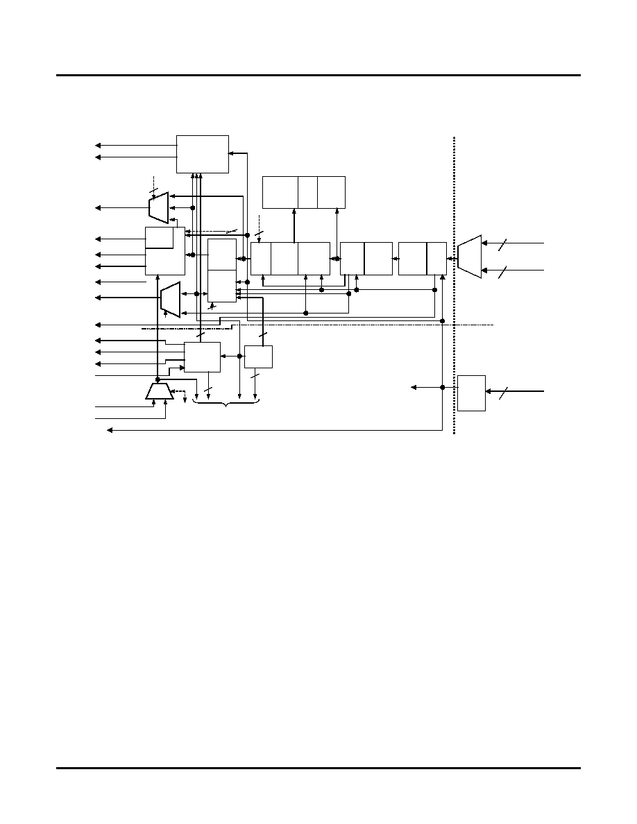
Figure 16. Basic Logic Blocks, Receive Path, Single Channel
HSI Functions (Clock Recovery and Deserializer)
The HSI receive path functions include Clock and Data Recovery (CDR) and deserialization of the incoming data
from the selected work or protect input stream to the byte-wide internal data bus format. The serial data received
from the LVDS buffer does not have an accompanying clock. Based on data transitions, the receiver selects an
appropriate internal clock phase for each channel to retime the data. The retimed data and clock are then passed
to the DEMUX (deserializer) module. The DEMUX module performs serial-to-parallel conversion and provides par-
allel data and clock to the SONET framer block. For a 622 Mbits/s SONET stream, the HSI will perform Clock and
Data Recovery (CDR) and MUX/DEMUX between 77.76 MHz byte-wide internal data buses and 622 Mbits/s serial
LVDS links.
Sampler
This block operates on the byte-wide data directly from the HSI macro. The HSI external interface always runs at
622 Mbits/s (STS-12), or 850 Mbits/s, but it can be connected directly to a 155 Mbits/s STS-3 stream. If connected
to a 155 Mbits/s stream, each incoming bit is received four times. This block is used to return the byte stream to the
expected STS-12 format. The mode of operation is controlled by a register and can either be STS-12 (pass-
through) or STS-3. The output from this block is not bit aligned (i.e., an 8-bit sample does not necessarily contain
an entire SONET byte), but it is in standard SONET STS-12 format (i.e., four STS-3s) and is suitable for framing.
SONET Framer Block
The framer block takes byte-wide data from the HSI, and outputs a byte-aligned, byte-wide data stream and 8 kHz
sync pulse. The framer algorithm determines the out-of-frame/in-frame status of the incoming data and will set
alarm register bits on both an errored frame and an Out-Of-Frame (OOF) state.
The framer block takes byte wide data from the HSI, and outputs a byte aligned byte wide stream and 8 kHz sync
pulse asserted coincident the rst A1 byte which will be used by following blocks. (Note however that if the pointer
Notes: n=[7,…0]
xx=[AA, AB,…BD]
* ~ Signal from Control
Register
FPF ~ Framer Frame Pulse
FPS ~ FIFO Sync Frame Pulse
LOF~ Loss of Frame
FPGA
Logic
Embedded Core
Backplane
Serial
Link
DOUTxx_PAR
CDR_CLK_xx
2
RXDxx_W_[P:N]
RXDxx_P_[P:N]
2
MUX
Logic Common
to Both Quads
To other
7 channels
2
LVDS
Buffer
To other
7 channels
SYS_FP
LINE_FP
FPGA_SYSCLK
TOH_CLK
SONET Logic
I/O
MUXs
And
LVDS
Buffers
SYS_CLK_[P:N]
TOH Data
Parallel to
Serial
Convert
Serial
To
Parallel
CDR
De-
Scrambler
(opt.)
Old B1
Read
(opt.)
AIS
Insert
New B1
Calc.
B1 Check
(opt.)
Prev.
B1
Pointer
Mover
(opt.)
Parity
Gen.
DOUTxx_SPE
DOUTxx_C1J1
DOUTxx[7:0]
MUX
Framer
(opt.)
Sampler
(for
STS3)
DOUTxx_EN
RX_TOH_CK_EN
RX_TOH_FP
TOH_CK_LP_EN
TOH_OUTxx
TOH_xx _EN
Align.
FIFO
(opt.)
FIFO
W/R
Control
DOUTxx _FP
TOH
Port
Control
FIFO
Sync.
FPF
*
LOF
FPS
Control and
TOH Clock
Recovered 77.76 MHz
77.76 MHz
MUX
Control and
TOH Clock
Bypass Align*
Bypass Mover*
2
Insert AIS-L*
Insert AIS-L
on LOF*
2
Line Lbk.*
Insert Bus
Par. Err.*
K1/K2 Pass
/Regen*
STS 12/48*
3
Min/Max Th.*
2
FIFO
Control
FIFO
Control
相關(guān)PDF資料 |
PDF描述 |
|---|---|
| P1010PSE5HFA | MPU PROTO 800/667 425-TEPBGA1 |
| P1013NXN2LFB | IC MPU 1067MHZ 689TEPBGA |
| P1013PSE2EFA | IC MPU PROTO 600MHZ 689-TEPBGA |
| P1014NSN5DFA | IC MPU 800MHZ 425TEPBGA1 |
| P1014NSN5FFA | IC MPU 800MHZ 425TEPBGA1 |
相關(guān)代理商/技術(shù)參數(shù) |
參數(shù)描述 |
|---|---|
| ORT8850L-3BMN680C | 功能描述:FPGA - 現(xiàn)場可編程門陣列 4992 LUT 278 I/O RoHS:否 制造商:Altera Corporation 系列:Cyclone V E 柵極數(shù)量: 邏輯塊數(shù)量:943 內(nèi)嵌式塊RAM - EBR:1956 kbit 輸入/輸出端數(shù)量:128 最大工作頻率:800 MHz 工作電源電壓:1.1 V 最大工作溫度:+ 70 C 安裝風格:SMD/SMT 封裝 / 箱體:FBGA-256 |
| ORT9303 | 制造商:BOT 制造商全稱:Bedford Opto Technology Ltd. 功能描述:3 ELEMENT PCB MOUNT 1.8mm LED ARRAY |
| ORT9303B | 制造商:BOT 制造商全稱:Bedford Opto Technology Ltd. 功能描述:3 ELEMENT PCB MOUNT 1.8mm LED ARRAY |
| ORT9303BL | 制造商:BOT 制造商全稱:Bedford Opto Technology Ltd. 功能描述:3 ELEMENT PCB MOUNT 1.8mm LED ARRAY |
| ORT9303G | 制造商:BOT 制造商全稱:Bedford Opto Technology Ltd. 功能描述:3 ELEMENT PCB MOUNT 1.8mm LED ARRAY |
發(fā)布緊急采購,3分鐘左右您將得到回復。