- 您現(xiàn)在的位置:買賣IC網(wǎng) > PDF目錄1958 > ORT8850L-3BM680C (Lattice Semiconductor Corporation)IC FPSC TRANSCEIVER 8CH 680-BGA PDF資料下載
參數(shù)資料
| 型號: | ORT8850L-3BM680C |
| 廠商: | Lattice Semiconductor Corporation |
| 文件頁數(shù): | 21/105頁 |
| 文件大?。?/td> | 0K |
| 描述: | IC FPSC TRANSCEIVER 8CH 680-BGA |
| 產(chǎn)品變化通告: | Product Discontinuation 01/Aug/2011 |
| 標準包裝: | 24 |
| 系列: | * |
第1頁第2頁第3頁第4頁第5頁第6頁第7頁第8頁第9頁第10頁第11頁第12頁第13頁第14頁第15頁第16頁第17頁第18頁第19頁第20頁當前第21頁第22頁第23頁第24頁第25頁第26頁第27頁第28頁第29頁第30頁第31頁第32頁第33頁第34頁第35頁第36頁第37頁第38頁第39頁第40頁第41頁第42頁第43頁第44頁第45頁第46頁第47頁第48頁第49頁第50頁第51頁第52頁第53頁第54頁第55頁第56頁第57頁第58頁第59頁第60頁第61頁第62頁第63頁第64頁第65頁第66頁第67頁第68頁第69頁第70頁第71頁第72頁第73頁第74頁第75頁第76頁第77頁第78頁第79頁第80頁第81頁第82頁第83頁第84頁第85頁第86頁第87頁第88頁第89頁第90頁第91頁第92頁第93頁第94頁第95頁第96頁第97頁第98頁第99頁第100頁第101頁第102頁第103頁第104頁第105頁
Lattice Semiconductor
ORCA ORT8850 Data Sheet
22
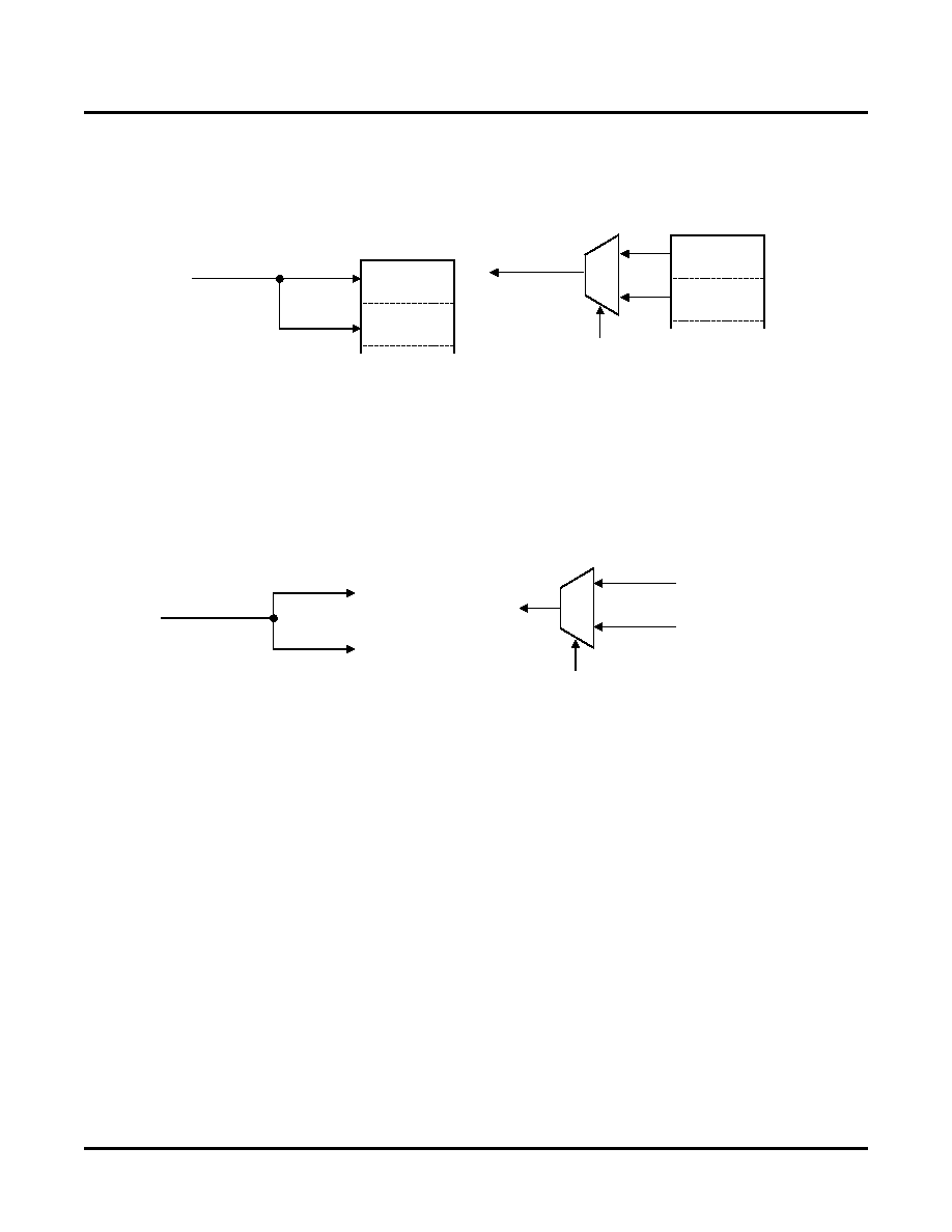
AA. This same scheme is used for channels groupings of AC/AD, BA/BB, and BC/BD. For quad protection when the
alignment FIFOs are to be used, the protection switching must be done in FPGA logic.
Figure 9. Parallel Protection Switching
LVDS protection switching (Figure 10) takes place at the LVDS buffer before the serial data is sent into the CDR.
The selection is between the main LVDS buffer and the protect LVDS buffer. The main LVDS buffer provide the
main receive data on RXDxx_W_[P:N] while the protect LVDS buffers provide protection receive data on
RXDxx_P_[P:N]. When operating using the main LVDS buffers (default) no status information is available on the
protect LVDS buffers since the serial stream must reach the SONET framer before status information is available
on the data stream. The same is also true for the main LVDS buffers when operating with the protect buffers.
Figure 10. LVDS Protection Switching
See Table 17 and Table 18 and the accompanying text for details and register settings for the protection switching
options.
FPSC Conguration - Overview
Conguration of the ORT8850 occurs in two stages: FPGA bit stream conguration and embedded core setup.
FPGA Conguration - Overview
Prior to becoming operational, the FPGA goes through a sequence of states, including power-up, initialization, con-
guration, start-up, and operation. The FPGA logic is congured by the standard FPGA bit stream conguration
means as discussed in the Series 4 FPGA data sheet. The options for the embedded core are set via registers that
are accessed through the FPGA system bus. The system bus can be driven by an external PPC compliant micro-
processor via the MPI block or via a user master interface in FPGA logic. A simple IP block, that drives the system
by using the user interface and uses very little FPGA logic, is available in the
MPI/System Bus technical note
(TN1017). This IP block sets up the embedded core via a state machine and allows the ORT8850 to work in an
independent system without an external MicroProcessor Interface.
Embedded Core Setup
All options for the operation of the core are congured according to the memory map shown in Table 19.
During the power-up sequence, the ORT8850 device (FPGA programmable circuit and the core) is held in reset. All
the LVDS output buffers and other output buffers are held in 3-state. All Flip-Flops in the core area are in reset
state, with the exception of the boundry-scan shift registers, which can only be reset by boundary-scan reset. After
power-up reset, the FPGA can start conguration. During FPGA conguration, the ORT8850 core will be held in
Work
Protect
Parallel TX Data
(From FPGA)
Transmit
Channel AA
Channel AB
Etc.
SONET and
HSI Blocks
Protect
Work/Protect Select
Receive
Parallel RX Data
(To FPGA)
Channel AA
Channel AB
Etc.
SONET and
HSI Blocks
Work
Work (to Work LVDS Buffer)
Protect (to Protect LVDS Buffer)
From TX SERDES
Transmit
Work (from Work LVDS Buffer)
Protect (from Protect LVDS Buffer)
Work/Protect Select
To CDR
Receive
相關(guān)PDF資料 |
PDF描述 |
|---|---|
| P1010PSE5HFA | MPU PROTO 800/667 425-TEPBGA1 |
| P1013NXN2LFB | IC MPU 1067MHZ 689TEPBGA |
| P1013PSE2EFA | IC MPU PROTO 600MHZ 689-TEPBGA |
| P1014NSN5DFA | IC MPU 800MHZ 425TEPBGA1 |
| P1014NSN5FFA | IC MPU 800MHZ 425TEPBGA1 |
相關(guān)代理商/技術(shù)參數(shù) |
參數(shù)描述 |
|---|---|
| ORT8850L-3BMN680C | 功能描述:FPGA - 現(xiàn)場可編程門陣列 4992 LUT 278 I/O RoHS:否 制造商:Altera Corporation 系列:Cyclone V E 柵極數(shù)量: 邏輯塊數(shù)量:943 內(nèi)嵌式塊RAM - EBR:1956 kbit 輸入/輸出端數(shù)量:128 最大工作頻率:800 MHz 工作電源電壓:1.1 V 最大工作溫度:+ 70 C 安裝風格:SMD/SMT 封裝 / 箱體:FBGA-256 |
| ORT9303 | 制造商:BOT 制造商全稱:Bedford Opto Technology Ltd. 功能描述:3 ELEMENT PCB MOUNT 1.8mm LED ARRAY |
| ORT9303B | 制造商:BOT 制造商全稱:Bedford Opto Technology Ltd. 功能描述:3 ELEMENT PCB MOUNT 1.8mm LED ARRAY |
| ORT9303BL | 制造商:BOT 制造商全稱:Bedford Opto Technology Ltd. 功能描述:3 ELEMENT PCB MOUNT 1.8mm LED ARRAY |
| ORT9303G | 制造商:BOT 制造商全稱:Bedford Opto Technology Ltd. 功能描述:3 ELEMENT PCB MOUNT 1.8mm LED ARRAY |
發(fā)布緊急采購,3分鐘左右您將得到回復(fù)。