- 您現(xiàn)在的位置:買賣IC網(wǎng) > PDF目錄98068 > S1C63653F 4-BIT, FLASH, 4 MHz, MICROCONTROLLER, CQFP100 PDF資料下載
參數(shù)資料
| 型號: | S1C63653F |
| 元件分類: | 微控制器/微處理器 |
| 英文描述: | 4-BIT, FLASH, 4 MHz, MICROCONTROLLER, CQFP100 |
| 封裝: | CERAMIC, QFP15-100 |
| 文件頁數(shù): | 21/121頁 |
| 文件大?。?/td> | 1127K |
| 代理商: | S1C63653F |
第1頁第2頁第3頁第4頁第5頁第6頁第7頁第8頁第9頁第10頁第11頁第12頁第13頁第14頁第15頁第16頁第17頁第18頁第19頁第20頁當(dāng)前第21頁第22頁第23頁第24頁第25頁第26頁第27頁第28頁第29頁第30頁第31頁第32頁第33頁第34頁第35頁第36頁第37頁第38頁第39頁第40頁第41頁第42頁第43頁第44頁第45頁第46頁第47頁第48頁第49頁第50頁第51頁第52頁第53頁第54頁第55頁第56頁第57頁第58頁第59頁第60頁第61頁第62頁第63頁第64頁第65頁第66頁第67頁第68頁第69頁第70頁第71頁第72頁第73頁第74頁第75頁第76頁第77頁第78頁第79頁第80頁第81頁第82頁第83頁第84頁第85頁第86頁第87頁第88頁第89頁第90頁第91頁第92頁第93頁第94頁第95頁第96頁第97頁第98頁第99頁第100頁第101頁第102頁第103頁第104頁第105頁第106頁第107頁第108頁第109頁第110頁第111頁第112頁第113頁第114頁第115頁第116頁第117頁第118頁第119頁第120頁第121頁
S1C63653 TECHNICAL MANUAL
EPSON
109
CHAPTER 5: SUMMARY OF NOTES
<R/f Converter>
● The power supply terminals for the analog system should be connected as shown below even if the
R/f converter is not used.
VDDA
→ VDD
VSSA
→ VSS
<Arrangement of Signal Lines>
● In order to prevent generation of electromagnetic induction noise caused by mutual inductance, do
not arrange a large current signal line near the circuits that are sensitive to noise such as the oscillation
unit and analog input unit.
● When a signal line is parallel with a high-speed line in long distance
or intersects a high-speed line, noise may generated by mutual
interference between the signals and it may cause a malfunction.
Do not arrange a high-speed signal line especially near circuits that
are sensitive to noise such as the oscillation unit and analog input unit.
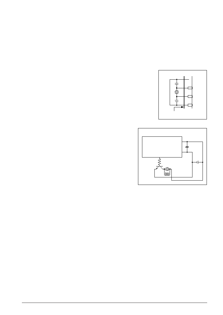
<Output Terminals>
● When an output terminal is used to drive an external
component that consumes a large amount of current, the
operation of the external component affects the built-in
power supply circuit of this IC and the output voltage may
vary. When driving a bipolar transistor by a periodic signal
such as the BZ or timer output in particular, it may cause
variations in the voltage output from the LCD system
voltage circuit that affects the contrast of the LCD display.
To prevent this, separate the traces on the printed circuit
board. Put one between the power supply and the IC's VDD
and VSS terminals, and another between the power supply
and the external component that consumes the large
amount of current. Furthermore, use an external compo-
nent with as low a current consumption as possible.
<Precautions for Visible Radiation (when bare chip is mounted)>
● Visible radiation causes semiconductor devices to change the electrical characteristics. It may cause
this IC to malfunction. When developing products which use this IC, consider the following precau-
tions to prevent malfunctions caused by visible radiations.
(1) Design the product and implement the IC on the board so that it is shielded from visible radiation
in actual use.
(2) The inspection process of the product needs an environment that shields the IC from visible
radiation.
(3) As well as the face of the IC, shield the back and side too.
OSC4
OSC3
VSS
Large current signal line
High-speed signal line
Prohibited pattern example
VDD
VSS
Piezo
BZ
CP
Example: Buzzer output circuit
+
相關(guān)PDF資料 |
PDF描述 |
|---|---|
| S1C6F567D0A0100 | MICROCONTROLLER, UUC141 |
| S1C6N3B0D0A0100 | MICROCONTROLLER, UUC54 |
| S1C6P366D0A0100 | 4-BIT, FLASH, 4.1 MHz, MICROCONTROLLER, UUC102 |
| S1C6P466D0A0A00 | MICROCONTROLLER, UUC140 |
| S1C6S2L7D | 4-BIT, MROM, 0.032 MHz, MICROCONTROLLER, UUC58 |
相關(guān)代理商/技術(shù)參數(shù) |
參數(shù)描述 |
|---|---|
| S1C63656 | 制造商:EPSON 制造商全稱:EPSON 功能描述:4-bit Single Chip Microcomputer |
| S1C63657 | 制造商:EPSON 制造商全稱:EPSON 功能描述:CMOS 4-bit Single Chip Microcontroller |
| S1C63658 | 制造商:EPSON 制造商全稱:EPSON 功能描述:4-bit Single Chip Microcomputer |
| S1C63666 | 制造商:EPSON 制造商全稱:EPSON 功能描述:4-bit Single Chip Microcomputer |
| S1C63709 | 制造商:EPSON 制造商全稱:EPSON 功能描述:4-bit Single Chip Microcomputer |
發(fā)布緊急采購,3分鐘左右您將得到回復(fù)。