- 您現(xiàn)在的位置:買賣IC網(wǎng) > PDF目錄373065 > K4N56163QF-GC (SAMSUNG SEMICONDUCTOR CO. LTD.) 256Mbit gDDR2 SDRAM PDF資料下載
參數(shù)資料
| 型號: | K4N56163QF-GC |
| 廠商: | SAMSUNG SEMICONDUCTOR CO. LTD. |
| 英文描述: | 256Mbit gDDR2 SDRAM |
| 中文描述: | 片256Mbit GDDR2 SDRAM的 |
| 文件頁數(shù): | 7/73頁 |
| 文件大小: | 1262K |
| 代理商: | K4N56163QF-GC |
第1頁第2頁第3頁第4頁第5頁第6頁當前第7頁第8頁第9頁第10頁第11頁第12頁第13頁第14頁第15頁第16頁第17頁第18頁第19頁第20頁第21頁第22頁第23頁第24頁第25頁第26頁第27頁第28頁第29頁第30頁第31頁第32頁第33頁第34頁第35頁第36頁第37頁第38頁第39頁第40頁第41頁第42頁第43頁第44頁第45頁第46頁第47頁第48頁第49頁第50頁第51頁第52頁第53頁第54頁第55頁第56頁第57頁第58頁第59頁第60頁第61頁第62頁第63頁第64頁第65頁第66頁第67頁第68頁第69頁第70頁第71頁第72頁第73頁
- 7 -
Rev 1.6 (Apr. 2005)
256M gDDR2 SDRAM
K4N56163QF-GC
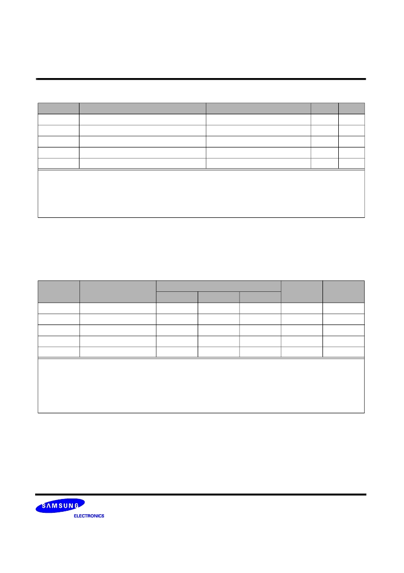
Absolute Maximum DC Ratings
AC & DC Operating Conditions
Recommended DC Operating Conditions (SSTL - 1.8)
Symbol
Parameter
Rating
Units
Notes
VDD
Voltage on VDD pin relative to Vss
- 1.0 V ~ 2.3 V
V
1
VDDQ
Voltage on VDDQ pin relative to Vss
- 0.5 V ~ 2.3 V
V
1
VDDL
Voltage on VDDL pin relative to Vss
- 0.5 V ~ 2.3 V
V
1
V
IN,
V
OUT
Voltage on any pin relative to Vss
- 0.5 V ~ 2.3 V
V
1
T
STG
Storage Temperature
-55 to +100
°
C
1, 2
1.
Stresses greater than those listed under “Absolute Maximum Ratings” may cause permanent damage to the device. This is a
stress rating only and functional operation of the device at these or any other conditions above those indicated in the operational
sections of this specification is not implied. Exposure to absolute maximum rating conditions for extended periods may affect reli-
ability.
2. Storage Temperature is the case surface temperature on the center/top side of the DRAM. For the measurement conditions, please
refer to JESD51-2 standard.
Symbol
Parameter
Rating
Units
Notes
Min.
Typ.
Max.
VDD
Supply Voltage
1.7
1.8
1.9
V
VDDL
Supply Voltage for DLL
1.7
1.8
1.9
V
4
VDDQ
Supply Voltage for Output
1.7
1.8
1.9
V
4
VREF
Input Reference Voltage
0.49*VDDQ
0.50*VDDQ
0.51*VDDQ
mV
1,2
VTT
Termination Voltage
VREF-0.04
VREF
VREF+0.04
V
3
There is no specific device VDD supply voltage requirement for SSTL-1.8 compliance. However under all conditions VDDQ must
be less than or equal to VDD.
1. The value of VREF may be selected by the user to provide optimum noise margin in the system. Typically the value of VREF is
expected to be about 0.5 x VDDQ of the transmitting device and VREF is expected to track variations in VDDQ.
2. Peak to peak AC noise on VREF may not exceed +/-2% VREF(DC).
3. VTT of transmitting device must track VREF of receiving device.
4. AC parameters are measured with VDD, VDDQ and VDDDL tied together.
相關(guān)PDF資料 |
PDF描述 |
|---|---|
| K4N56163QF-GC25 | 256Mbit gDDR2 SDRAM |
| K4N56163QF-GC30 | 256Mbit gDDR2 SDRAM |
| K4N56163QF-GC37 | 256Mbit gDDR2 SDRAM |
| K4PE68A | Transient Voltage Suppressor Diodes |
| K4R271669A | 256K x 16/18 bit x 2*16 Dependent Banks Direct RDRAMTM |
相關(guān)代理商/技術(shù)參數(shù) |
參數(shù)描述 |
|---|---|
| K4N56163QF-GC25 | 制造商:SAMSUNG 制造商全稱:Samsung semiconductor 功能描述:256Mbit gDDR2 SDRAM |
| K4N56163QF-GC30 | 制造商:SAMSUNG 制造商全稱:Samsung semiconductor 功能描述:256Mbit gDDR2 SDRAM |
| K4N56163QF-GC37 | 制造商:SAMSUNG 制造商全稱:Samsung semiconductor 功能描述:256Mbit gDDR2 SDRAM |
| K4N56163QG-ZC2A | 制造商:Samsung Semiconductor 功能描述: |
| K4P24V3 | 制造商:AROMAT 功能描述:REPLAY 700 OHM |
發(fā)布緊急采購,3分鐘左右您將得到回復(fù)。