- 您現(xiàn)在的位置:買賣IC網(wǎng) > PDF目錄370499 > HDMP-1024 Low Cost Gigabit Rate Receive Chip Set with TTL I/Os(帶TTL輸入/輸出的低價格千兆位速率接收芯片) PDF資料下載
參數(shù)資料
| 型號: | HDMP-1024 |
| 英文描述: | Low Cost Gigabit Rate Receive Chip Set with TTL I/Os(帶TTL輸入/輸出的低價格千兆位速率接收芯片) |
| 中文描述: | 低成本千兆速率接收芯片組配備TTL的I / O(帶的TTL輸入/輸出的低價格千兆位速率接收芯片) |
| 文件頁數(shù): | 36/40頁 |
| 文件大小: | 363K |
| 代理商: | HDMP-1024 |
第1頁第2頁第3頁第4頁第5頁第6頁第7頁第8頁第9頁第10頁第11頁第12頁第13頁第14頁第15頁第16頁第17頁第18頁第19頁第20頁第21頁第22頁第23頁第24頁第25頁第26頁第27頁第28頁第29頁第30頁第31頁第32頁第33頁第34頁第35頁當前第36頁第37頁第38頁第39頁第40頁
36
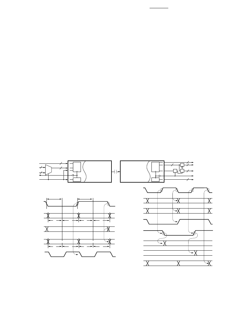
On the Tx side, the expected
frequency is 1/2 of the combined
frame period. This combined
frame, D0-D19, is formed by
interlacing the two frames C0-
C19 and C20-C39 with an
external 2:1 multiplexer. The Tx
locks onto STRBIN, which has the
same frequency as the bit rate of
C0-C39, and with an internal
frequency doubler, generates the
sampling clock to latch in
D0-D19, DAV*, CAV*, and FLAG.
STRBIN is also used to toggle the
2:1 multiplexer, and is fed into
the flag input to signify the two
frames. The setup and hold times
are referenced to 1/2 frame
period plus 4 ns of D0-D19, or 90
degrees, from the edges of
STRBIN. The multiplexer delay,
t
mux
, should be considered for
timing margins. The STRBOUT is
derived from the internal
sampling clock, and thus has a
frequency double that of STRBIN.
The falling edge of STRBOUT
appears after the rising and
falling edges of STRBIN after a
delay of T
strb
. Other interlacing
techniques can also be achieved
with edge-triggered latches for
improved timing margins.
In the Rx side, the frame D0-D19
are demultiplexed back to the
original C0-C19, and C20-C39
frames with the use of external
edge-triggered flip-flops. The
toggle clock of the flip-flops,
RCLK, is derived by the state of
the FLAG bit. RCLK toggles with
the rising edge of STRBOUT with
a delay of t
da
. The two frames
appear with the rising and falling
edges of RCLK with a delay of t
db
.
All of the synchronous outputs
and state machine outputs appear
after the falling edge of STRBOUT
with delays of t
d1
and t
d2
,
respectively.
The lower frame of C0-C19 can
be delayed further with additional
latches so that both C0-C19 and
C20-C39 frames are synchronous.
Supply Bypassing and
Integrator Capacitor
Figure 20 shows the location of
the PLL integrator capacitors,
power supply capacitors and
required grounding for the Tx and
Rx chips.
Figure 19. Transmitter and Receiver Data Interface and Timing for Double Frame Mode (MDFSEL=1).
Tx
CONFIGURATIONS
CAV*, DAV*
C00 - C19
PLL
STRBOUT
STRBIN
Rx
CONFIGURATIONS
CAV*, DAV*, FF
LINKRDY*, ERROR
C00 - C19
STRBOUT
STAT0; STAT1
t
s
t
h
t
strb
CAV*, DAV*
STRBOUT
STRBIN
FLAG
CAV*, DAV*
FF, LINKRDY*
ERROR
D00 - D19
STRBOUT
t
d1
t
s
= SETUP TIME
t
h
= HOLD TIME
t
strb
= STRBIN TO STRBOUT DELAY
t
mux
= 2:1 MULTIPLEXER DELAY
t
d1
= STRBOUT TO SYNCHRONOUS OUTPUTS DELAY
t
d2
= STRBOUT TO STATE MACHINE OUTPUTS DELAY
t
da
= STRBOUT TO RCLK DELAY
t
db
= RCLK TO C00-C39 OUTPUT DELAY
2:1
1
0
D00 - D19
C20 - C39
C20 - C39
D00 - D19
FLAG
FLAG
1/2 FRAME
PERIOD
1/2 FRAME
PERIOD
t
s
t
h
t
s
t
h
D00 - D19
t
s
t
h
C00 - C19
C20 - C39
C00 - C19
C20 - C39
t
mux
t
d2
STAT0
STAT1
FLAG
RCLK
C00 - C19
C20 - C39
C00 - C19
C20 - C39
t
da
t
da
t
db
t
db
RCLK
相關PDF資料 |
PDF描述 |
|---|---|
| HDMP-1032 | 1.4 GBd Transmitter Chip Set with CIMT Encoder/Decoder and Variable Data Rate(帶CIMT編碼器/譯碼器和變量數(shù)據(jù)速率的1.4 GBd 傳送器) |
| HDMP-1034 | 1.4 GBd Receiver Chip Set with CIMT Encoder/Decoder and Variable Data Rate(帶CIMT編碼器/譯碼器和變量數(shù)據(jù)速率的1.4 GBd 接收器) |
| HDMP-1512 | Fibre Channel Transmitter Chipset(光纖通道傳送芯片) |
| HDMP-1514 | Fibre Channel Receiver Chipset(光纖通道接收芯片) |
| HDMP-1526 | Transistor Diode Kit;Contents Of Kit:Transistor/Diode Kit |
相關代理商/技術參數(shù) |
參數(shù)描述 |
|---|---|
| HDMP-1032 | 制造商:AGILENT 制造商全稱:AGILENT 功能描述:1.4 GBd Transmitter/Receiver Chip Set with CIMT Encoder/Decoder and Variable Data Rate |
| HDMP-1032A | 制造商:未知廠家 制造商全稱:未知廠家 功能描述:1.4 GBd Transmitter Chip with CIMT Encoder/Decoder and Variable Data Rate |
| HDMP-1034 | 制造商:AGILENT 制造商全稱:AGILENT 功能描述:1.4 GBd Transmitter/Receiver Chip Set with CIMT Encoder/Decoder and Variable Data Rate |
| HDMP-1034A | 制造商:HP 制造商全稱:Agilent(Hewlett-Packard) 功能描述:Transmitter/Receiver Chip Set |
| HDMP-1512 | 制造商:AGILENT 制造商全稱:AGILENT 功能描述:Fibre Channel Transmitter and Receiver Chipset |
發(fā)布緊急采購,3分鐘左右您將得到回復。