- 您現(xiàn)在的位置:買賣IC網(wǎng) > PDF目錄370499 > HDMP-1024 Low Cost Gigabit Rate Receive Chip Set with TTL I/Os(帶TTL輸入/輸出的低價格千兆位速率接收芯片) PDF資料下載
參數(shù)資料
| 型號: | HDMP-1024 |
| 英文描述: | Low Cost Gigabit Rate Receive Chip Set with TTL I/Os(帶TTL輸入/輸出的低價格千兆位速率接收芯片) |
| 中文描述: | 低成本千兆速率接收芯片組配備TTL的I / O(帶的TTL輸入/輸出的低價格千兆位速率接收芯片) |
| 文件頁數(shù): | 16/40頁 |
| 文件大小: | 363K |
| 代理商: | HDMP-1024 |
第1頁第2頁第3頁第4頁第5頁第6頁第7頁第8頁第9頁第10頁第11頁第12頁第13頁第14頁第15頁當(dāng)前第16頁第17頁第18頁第19頁第20頁第21頁第22頁第23頁第24頁第25頁第26頁第27頁第28頁第29頁第30頁第31頁第32頁第33頁第34頁第35頁第36頁第37頁第38頁第39頁第40頁
16
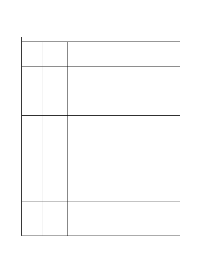
Tx I/O Definition (cont’d.)
Name
EHCLKSEL
Pin
78
Type
I-TTL
Signal
EHCLK Enable:
When active, this input causes the STRBIN inputs
to be used for the transmit serial clock, rather than the internal VCO
clock. When the STRBIN is active, it is necessary for the data source to take
its clock from the link rather than the usual operation where the link
phase-locks onto the data source clock.This clock replaces the internal VCO
clock and is intended for diagnostic purposes only.
Fill Frame Select:
When neither CAV* or DAV* is asserted, or when
ED is false, fill frames are automatically transmitted to allow the Rx
chip to maintain lock. The type of fill frame sent is determined by
the state of this pin. FF0s are sent if low, and either FF1a or FF1b is
sent if FF is high. The choice of FF1a and FF1b is determined by the
state of the cumulative line DC balance.
Extra Flag Bit:
When FLAGSEL is active, this input is sent as an
extra data bit in addition to the normal Data inputs. When FLAGSEL
is not asserted, this input is ignored and the transmitted Flag bit is
internally alternated to allow the Rx chip to perform enhanced frame
error detection. FLAG is not available as a data bit when a control
word is transmitted.
Flag Bit Mode Select:
When this input is high, the extra FLAG bit
input is sent as an extra transparent data bit. Otherwise, the FLAG
input is ignored and the transmitted flag bit is internally alternated
by the transmitter. The Rx chip can provide enhanced frame error
detection by checking for strict alternation of the flag bit during data
frames. The FLAGSEL input on the Rx chip must be set to the same
value as the Tx FLAGSEL input.
TTL Ground:
Normally 0 Volts. Tie to ground.
FF
68
I-TTL
FLAG
60
I-TTL
FLAGSEL
71
I-TTL
GND
TTL
26
80
5
6
9
21
22
28
29
30
41
42
61
62
11
12
S
GND
S
Ground:
Normally 0 Volts. Tie to ground.
HCLK
HCLK*
O-BLL
High Speed Clock Monitor:
Used to monitor actual clock signal
used to transmit the serial data. This signal will either be the divided
VCO output, or the divided EHCLK external clock input, depending
on the value of the EHCLKSEL input.
HCLK Power-down Control:
When this pin is de-asserted, the HCLK,
HCLK* outputs are powered down to reduce power dissipation.
Invert Signal:
A high value of INV implies that the current frame is
being sent inverted to maintain long-term DC balance.
HCLKON
10
I-TTL
INV
25
O-TTL
相關(guān)PDF資料 |
PDF描述 |
|---|---|
| HDMP-1032 | 1.4 GBd Transmitter Chip Set with CIMT Encoder/Decoder and Variable Data Rate(帶CIMT編碼器/譯碼器和變量數(shù)據(jù)速率的1.4 GBd 傳送器) |
| HDMP-1034 | 1.4 GBd Receiver Chip Set with CIMT Encoder/Decoder and Variable Data Rate(帶CIMT編碼器/譯碼器和變量數(shù)據(jù)速率的1.4 GBd 接收器) |
| HDMP-1512 | Fibre Channel Transmitter Chipset(光纖通道傳送芯片) |
| HDMP-1514 | Fibre Channel Receiver Chipset(光纖通道接收芯片) |
| HDMP-1526 | Transistor Diode Kit;Contents Of Kit:Transistor/Diode Kit |
相關(guān)代理商/技術(shù)參數(shù) |
參數(shù)描述 |
|---|---|
| HDMP-1032 | 制造商:AGILENT 制造商全稱:AGILENT 功能描述:1.4 GBd Transmitter/Receiver Chip Set with CIMT Encoder/Decoder and Variable Data Rate |
| HDMP-1032A | 制造商:未知廠家 制造商全稱:未知廠家 功能描述:1.4 GBd Transmitter Chip with CIMT Encoder/Decoder and Variable Data Rate |
| HDMP-1034 | 制造商:AGILENT 制造商全稱:AGILENT 功能描述:1.4 GBd Transmitter/Receiver Chip Set with CIMT Encoder/Decoder and Variable Data Rate |
| HDMP-1034A | 制造商:HP 制造商全稱:Agilent(Hewlett-Packard) 功能描述:Transmitter/Receiver Chip Set |
| HDMP-1512 | 制造商:AGILENT 制造商全稱:AGILENT 功能描述:Fibre Channel Transmitter and Receiver Chipset |
發(fā)布緊急采購,3分鐘左右您將得到回復(fù)。