- 您現(xiàn)在的位置:買賣IC網(wǎng) > PDF目錄15530 > EVAL-ADUC7023QSPZ1 (Analog Devices Inc)BOARD EVAL FOR ADUC7023 PDF資料下載
參數(shù)資料
| 型號: | EVAL-ADUC7023QSPZ1 |
| 廠商: | Analog Devices Inc |
| 文件頁數(shù): | 87/96頁 |
| 文件大小: | 0K |
| 描述: | BOARD EVAL FOR ADUC7023 |
| 標(biāo)準(zhǔn)包裝: | 1 |
| 系列: | QuickStart™ PLUS 套件 |
| 類型: | MCU |
| 適用于相關(guān)產(chǎn)品: | ADuC7023 |
| 所含物品: | 板 |
第1頁第2頁第3頁第4頁第5頁第6頁第7頁第8頁第9頁第10頁第11頁第12頁第13頁第14頁第15頁第16頁第17頁第18頁第19頁第20頁第21頁第22頁第23頁第24頁第25頁第26頁第27頁第28頁第29頁第30頁第31頁第32頁第33頁第34頁第35頁第36頁第37頁第38頁第39頁第40頁第41頁第42頁第43頁第44頁第45頁第46頁第47頁第48頁第49頁第50頁第51頁第52頁第53頁第54頁第55頁第56頁第57頁第58頁第59頁第60頁第61頁第62頁第63頁第64頁第65頁第66頁第67頁第68頁第69頁第70頁第71頁第72頁第73頁第74頁第75頁第76頁第77頁第78頁第79頁第80頁第81頁第82頁第83頁第84頁第85頁第86頁當(dāng)前第87頁第88頁第89頁第90頁第91頁第92頁第93頁第94頁第95頁第96頁
ADuC7023
Data Sheet
| Page 88 of 96
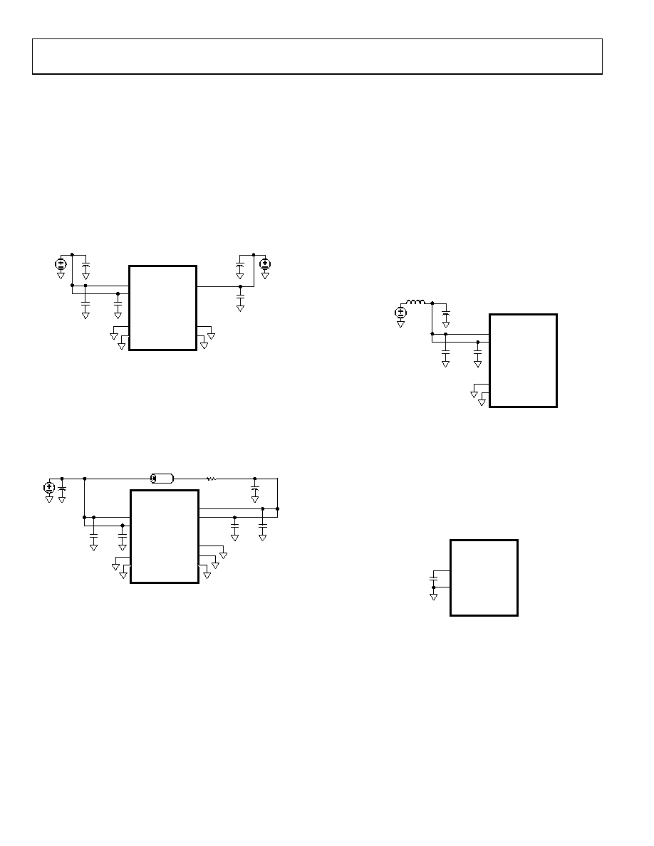
HARDWARE DESIGN CONSIDERATIONS
POWER SUPPLIES
The ADuC7023 operational power supply voltage range is 2.7 V
to 3.6 V. Separate analog and digital power supply pins (AVDD
and IOVDD, respectively) allow AVDD to be kept relatively free of
noisy digital signals often present on the system IOVDD line. In
this mode, the part can also operate with split supplies, that is, it
can use different voltage levels for each supply. For example, the
system can be designed to operate with an IOVDD voltage level
of 3.3 V while the AVDD level can be at 3 V, or vice versa. A
typical split supply configuration is shown in Figure 46.
08675-
041
ADuC7023
IOVDD
AVDD
GNDREF
AGND
IOGND
0.1F
10F
DIGITAL SUPPLY
ANALOG SUPPLY
Figure 46. External Dual Supply Connections
As an alternative to providing two separate power supplies, the
user can reduce noise on AVDD by placing a small series resistor
and/or ferrite bead between AVDD and IOVDD, and then decoupling
AVDD separately to ground. An example of this configuration is
shown in Figure 47. With this configuration, other analog circuitry
(such as op amps, voltage reference, and others) can be powered
from the AVDD supply line as well.
08675-
054
ADuC7023
IOVDD
AVDD
GNDREF
AGND
REFGND
IOGND
0.1F
1.6V
10F
0.1F
DIGITAL SUPPLY
BEAD
10F
Figure 47. External Single Supply Connections
In both Figure 46 and Figure 47, a large value (10 F) reservoir
capacitor sits on IOVDD, and a separate 10 F capacitor sits on
AVDD. In addition, local small-value (0.1 F) capacitors are located
at each AVDD and IOVDD pin of the chip. As per standard design
practice, include all of these capacitors and ensure the smaller
capacitors are close to each AVDD pin with trace lengths as
short as possible. Connect the ground terminal of each of
these capacitors directly to the underlying ground plane.
Finally, the analog and digital ground pins on the ADuC7023
must be referenced to the same system ground reference point
at all times.
IOVDD Supply Sensitivity
The IOVDD supply is sensitive to high frequency noise because it
is the supply source for the internal oscillator and PLL circuits.
When the internal PLL loses lock, the clock source is removed
by a gating circuit from the CPU, and the ARM7TDMI core
stops executing code until the PLL regains lock. This feature is
to ensure that no flash interface timings or ARM7TDMI
timings are violated.
Typically, frequency noise greater than 50 kHz and 50 mV p-p
on top of the supply causes the core to stop working.
If decoupling values recommended in the Power Supplies section
do not sufficiently dampen all noise soures below 50 mV on IOVDD,
a filter such as the one shown in Figure 48 is recommended.
08675-
042
ADuC7023
IOVDD
IOGND
0.1F
10F
1H
DIGITAL
SUPPLY
Figure 48. Recommended IOVDD Supply Filter
Linear Voltage Regulator
Each ADuC7023 requires a single 3.3 V supply, but the core
logic requires a 2.6 V supply. An on-chip linear regulator generates
the 2.6 V from IOVDD for the core logic. The LVDD pin is the 2.6 V
supply for the core logic. An external compensation capacitor of
0.47 F must be connected between LVDD and DGND (as close
as possible to these pins) to act as a tank of charge, as shown in
08675-
043
ADuC7023
LVDD
DGND
0.47F
Figure 49. Voltage Regulator Connections
The LVDD pin should not be used for any other chip. It is also
recommended to use excellent power supply decoupling on
IOVDD to help improve line regulation performance of the
on-chip voltage regulator.
Rev. E
相關(guān)PDF資料 |
PDF描述 |
|---|---|
| AIUR-10-182K | INDUCTOR POWER 1800UH 10% T/H |
| EYM15DRSD | CONN EDGECARD 30POS DIP .156 SLD |
| V300C3V3C50B | CONVERTER MOD DC/DC 3.3V 50W |
| AIUR-06-271K | INDUCTOR POWER 270UH 10% T/H |
| EGM15DRSD | CONN EDGECARD 30POS DIP .156 SLD |
相關(guān)代理商/技術(shù)參數(shù) |
參數(shù)描述 |
|---|---|
| EVAL-ADuC7023QSPZ2 | 制造商:AD 制造商全稱:Analog Devices 功能描述:Precision Analog Microcontroller, 12-Bit Analog I/O, ARM7TDMI MCU with Enhanced IRQ Handler |
| EVALADUC7023QSPZU1 | 制造商:Analog Devices 功能描述: |
| EVAL-ADUC7024QS | 制造商:Analog Devices 功能描述:QUICK START DEVELOPMENT SYSTEM - Bulk |
| EVAL-ADUC7024QS-U2 | 制造商:Analog Devices 功能描述:QUICK START DEVL SYST EVAL BOARD I.C. - Bulk |
| EVAL-ADUC7024QS-U3 | 制造商:Analog Devices 功能描述:ARM7 ADUC7024 QUICKSTART DEV KIT |
發(fā)布緊急采購,3分鐘左右您將得到回復(fù)。