- 您現(xiàn)在的位置:買賣IC網(wǎng) > PDF目錄15530 > EVAL-ADUC7023QSPZ1 (Analog Devices Inc)BOARD EVAL FOR ADUC7023 PDF資料下載
參數(shù)資料
| 型號: | EVAL-ADUC7023QSPZ1 |
| 廠商: | Analog Devices Inc |
| 文件頁數(shù): | 64/96頁 |
| 文件大?。?/td> | 0K |
| 描述: | BOARD EVAL FOR ADUC7023 |
| 標(biāo)準(zhǔn)包裝: | 1 |
| 系列: | QuickStart™ PLUS 套件 |
| 類型: | MCU |
| 適用于相關(guān)產(chǎn)品: | ADuC7023 |
| 所含物品: | 板 |
第1頁第2頁第3頁第4頁第5頁第6頁第7頁第8頁第9頁第10頁第11頁第12頁第13頁第14頁第15頁第16頁第17頁第18頁第19頁第20頁第21頁第22頁第23頁第24頁第25頁第26頁第27頁第28頁第29頁第30頁第31頁第32頁第33頁第34頁第35頁第36頁第37頁第38頁第39頁第40頁第41頁第42頁第43頁第44頁第45頁第46頁第47頁第48頁第49頁第50頁第51頁第52頁第53頁第54頁第55頁第56頁第57頁第58頁第59頁第60頁第61頁第62頁第63頁當(dāng)前第64頁第65頁第66頁第67頁第68頁第69頁第70頁第71頁第72頁第73頁第74頁第75頁第76頁第77頁第78頁第79頁第80頁第81頁第82頁第83頁第84頁第85頁第86頁第87頁第88頁第89頁第90頁第91頁第92頁第93頁第94頁第95頁第96頁
Data Sheet
ADuC7023
| Page 67 of 96
Table 74. I2CxFSTA MMR Bit Designations
Bit
Name
Description
15 to 10
Reserved bits.
9
I2CFMTX
This bit is set to 1 to flush the master
Tx FIFO.
8
I2CFSTX
This bit is set to 1 to flush the slave Tx
FIFO.
7 to 6
I2CMRXSTA
I2C master receive FIFO status bits.
[00] = FIFO empty.
[01] = byte written to FIFO.
[10] = 1 byte in FIFO.
[11] = FIFO full.
5 to 4
I2CMTXSTA
I2C master transmit FIFO status bits.
[00] = FIFO empty.
[01] = byte written to FIFO.
[10] = 1 byte in FIFO.
[11] = FIFO full.
3 to 2
I2CSRXSTA
I2C slave receive FIFO status bits.
[00] = FIFO empty
[01] = byte written to FIFO
[10] = 1 byte in FIFO
[11] = FIFO full
1 to 0
I2CSTXSTA
I2C slave transmit FIFO status bits.
[00] = FIFO empty.
[01] = byte written to FIFO.
[10] = 1 byte in FIFO.
[11] = FIFO full.
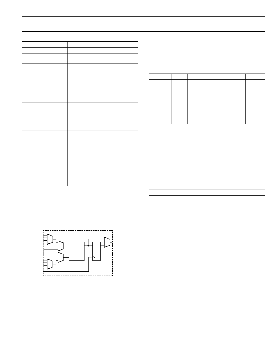
PROGRAMMABLE LOGIC ARRAY (PLA)
Every ADuC7023 integrates a fully programmable logic array
(PLA) consisting of sixteen PLA elements.
Each PLA element contains a two-input look-up table that can
be configured to generate any logic output function based on
two inputs and a flip-flop. This is represented in Figure 39.
08675-
033
4
2
0
1
3
A
B
LOOK-UP
TABLE
Figure 39. PLA Element
In total, 20 GPIO pins are available on the ADuC7023 for the
PLA. These include 11 input pins and nine output pins, which
need to be configured in the GPxCON register as PLA pins before
using the PLA.
The PLA is configured via a set of user MMRs. The output(s) of
the PLA can be routed to the internal interrupt system, to the
CONVSTART signal of the ADC, to an MMR, or to any of the
eight PLA output pins.
Table 75. Element Input/Output
PLA Block 0
PLA Block 1
Element
Input
Output
Element
Input
Output
0
P0.4
P0.7
8
P0.0
P0.2
1
P0.5
P1.0
9
P0.1
P0.3
2
P0.6
P1.1
10
P2.4
P2.51
3
P1.2
P1.4
11
NC
4
P1.3
P1.5
12
NC
5
P1.6
P2.11
13
NC
6
P1.7
P2.2
14
NC
7
P2.0
P2.3
15
NC
1
Internal pins only. Read via GPxDAT register.
PLA MMRs Interface
The PLA peripheral interface consists of the 22 MMRs
described in the following sections.
PLAELMx Registers
PLAELMx are Element 0 to Element 15 control registers. They
configure the input and output mux of each element, select the
function in the look-up table, and bypass/use the flip-flop (see
Table 76. PLAELMx Registers
Name
Address
Default Value
Access
PLAELM0
0xFFFF0B00
0x0000
R/W
PLAELM1
0xFFFF0B04
0x0000
R/W
PLAELM2
0xFFFF0B08
0x0000
R/W
PLAELM3
0xFFFF0B0C
0x0000
R/W
PLAELM4
0xFFFF0B10
0x0000
R/W
PLAELM5
0xFFFF0B14
0x0000
R/W
PLAELM6
0xFFFF0B18
0x0000
R/W
PLAELM7
0xFFFF0B1C
0x0000
R/W
PLAELM8
0xFFFF0B20
0x0000
R/W
PLAELM9
0xFFFF0B24
0x0000
R/W
PLAELM10
0xFFFF0B28
0x0000
R/W
PLAELM11
0xFFFF0B2C
0x0000
R/W
PLAELM12
0xFFFF0B30
0x0000
R/W
PLAELM13
0xFFFF0B34
0x0000
R/W
PLAELM14
0xFFFF0B38
0x0000
R/W
PLAELM15
0xFFFF0B3C
0x0000
R/W
Rev. E
相關(guān)PDF資料 |
PDF描述 |
|---|---|
| AIUR-10-182K | INDUCTOR POWER 1800UH 10% T/H |
| EYM15DRSD | CONN EDGECARD 30POS DIP .156 SLD |
| V300C3V3C50B | CONVERTER MOD DC/DC 3.3V 50W |
| AIUR-06-271K | INDUCTOR POWER 270UH 10% T/H |
| EGM15DRSD | CONN EDGECARD 30POS DIP .156 SLD |
相關(guān)代理商/技術(shù)參數(shù) |
參數(shù)描述 |
|---|---|
| EVAL-ADuC7023QSPZ2 | 制造商:AD 制造商全稱:Analog Devices 功能描述:Precision Analog Microcontroller, 12-Bit Analog I/O, ARM7TDMI MCU with Enhanced IRQ Handler |
| EVALADUC7023QSPZU1 | 制造商:Analog Devices 功能描述: |
| EVAL-ADUC7024QS | 制造商:Analog Devices 功能描述:QUICK START DEVELOPMENT SYSTEM - Bulk |
| EVAL-ADUC7024QS-U2 | 制造商:Analog Devices 功能描述:QUICK START DEVL SYST EVAL BOARD I.C. - Bulk |
| EVAL-ADUC7024QS-U3 | 制造商:Analog Devices 功能描述:ARM7 ADUC7024 QUICKSTART DEV KIT |
發(fā)布緊急采購,3分鐘左右您將得到回復(fù)。