- 您現(xiàn)在的位置:買賣IC網(wǎng) > PDF目錄1974 > XCF128XFTG64C (Xilinx Inc)IC PROM SRL 128M GATE 64-FTBGA PDF資料下載
參數(shù)資料
| 型號: | XCF128XFTG64C |
| 廠商: | Xilinx Inc |
| 文件頁數(shù): | 63/88頁 |
| 文件大小: | 0K |
| 描述: | IC PROM SRL 128M GATE 64-FTBGA |
| 標準包裝: | 1 |
| 可編程類型: | 系統(tǒng)內(nèi)可編程 |
| 存儲容量: | 128Mb |
| 電源電壓: | 1.7 V ~ 2 V |
| 工作溫度: | -40°C ~ 85°C |
| 封裝/外殼: | 64-TBGA |
| 供應(yīng)商設(shè)備封裝: | 64-TFBGA |
| 包裝: | 托盤 |
| 產(chǎn)品目錄頁面: | 601 (CN2011-ZH PDF) |
| 其它名稱: | 122-1578 |
第1頁第2頁第3頁第4頁第5頁第6頁第7頁第8頁第9頁第10頁第11頁第12頁第13頁第14頁第15頁第16頁第17頁第18頁第19頁第20頁第21頁第22頁第23頁第24頁第25頁第26頁第27頁第28頁第29頁第30頁第31頁第32頁第33頁第34頁第35頁第36頁第37頁第38頁第39頁第40頁第41頁第42頁第43頁第44頁第45頁第46頁第47頁第48頁第49頁第50頁第51頁第52頁第53頁第54頁第55頁第56頁第57頁第58頁第59頁第60頁第61頁第62頁當前第63頁第64頁第65頁第66頁第67頁第68頁第69頁第70頁第71頁第72頁第73頁第74頁第75頁第76頁第77頁第78頁第79頁第80頁第81頁第82頁第83頁第84頁第85頁第86頁第87頁第88頁
Platform Flash XL High-Density Configuration and Storage Device
DS617 (v3.0.1) January 07, 2010
Product Specification
66
R
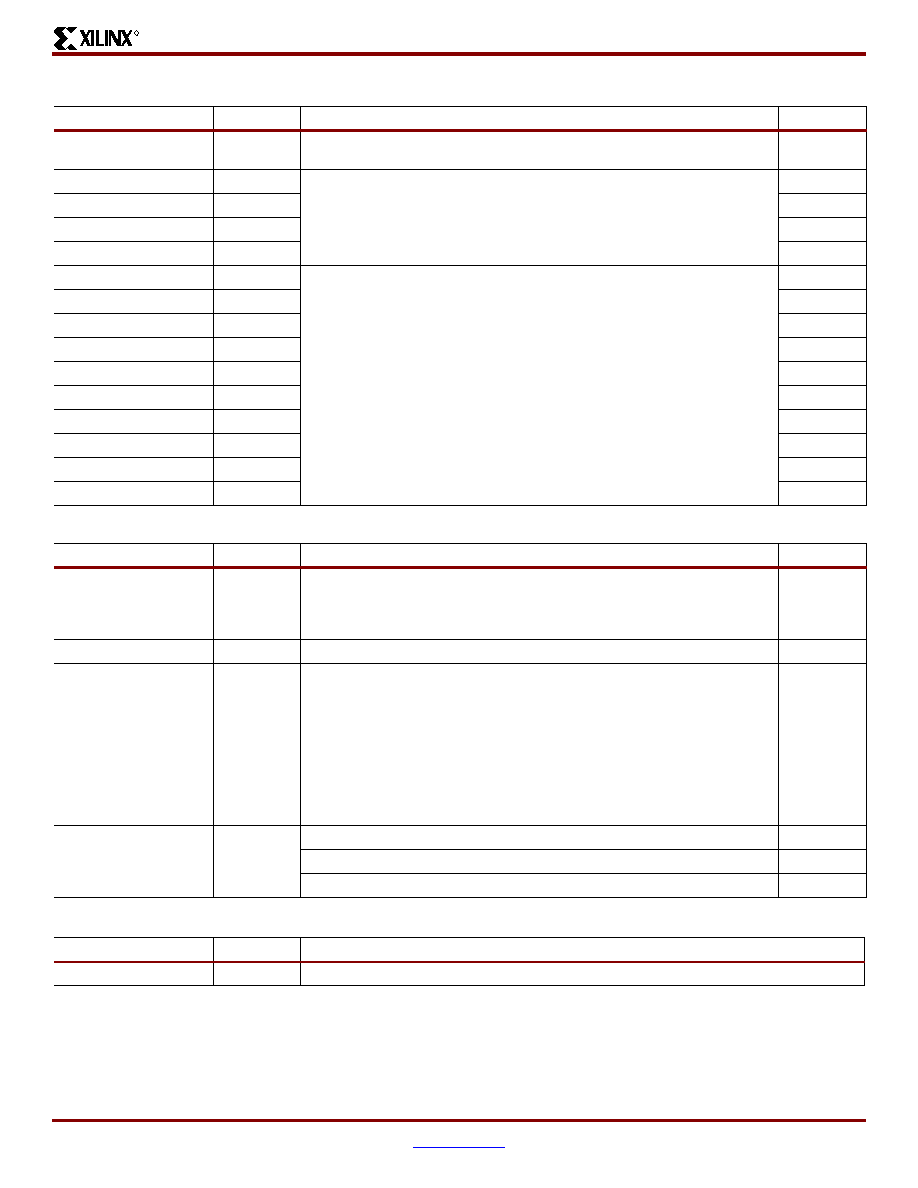
Table 41: Protection Register Information
Offset
Data
Description
Value
(P+E)h = 118h
0002h
Number of protection register fields in JEDEC ID space. 0000h indicates that
256 fields are available.
2
(P+F)h = 119h
0080h
Protection Register 1: Protection Description:
Bits 0-7 Lower byte of protection register address
Bits 8-15 Upper byte of protection register address
Bits 16-23 2n bytes in factory pre-programmed region
Bits 24-31 2n bytes in user programmable region
80h
(P+10)h = 11Ah
0000h
00h
(P+ 11)h = 11Bh
0003h
8 bytes
(P+12)h = 11Ch
0003h
8 bytes
(P+13)h = 11Dh
0089h
Protection Register 2: Protection Description:
Bits 0-31 protection register address
Bits 32-39 n number of factory programmed regions (lower byte)
Bits 40-47 n number of factory programmed regions (upper byte)
Bits 48-55 2n bytes in factory programmable region
Bits 56-63 n number of user programmable regions (lower byte)
Bits 64-71 n number of user programmable regions (upper byte)
Bits 72-79 2n bytes in user programmable region
89h
(P+14)h = 11Eh
0000h
00h
(P+15)h = 11Fh
0000h
00h
(P+16)h = 120h
0000h
00h
(P+17)h = 121h
0000h
0
(P+18)h = 122h
0000h
0
(P+19)h = 123h
0000h
0
(P+1A)h = 124h
0010h
16
(P+1B)h = 125h
0000h
0
(P+1C)h = 126h
0004h
16
Table 42: Burst Read Information
Offset
Data
Description
Value
(P+1D)h = 127h
0003h
Page-mode read capability
bits 0-7 n’ such that 2n HEX value represents the number of read-page
bytes. See offset 0028h for device word width to determine page-mode data
output width.
8 bytes
(P+1E)h = 128h
0004h
Number of synchronous mode read configuration fields that follow.
4
(P+1F)h = 129h
0001h
Synchronous mode read capability configuration 1
bit 3-7 Reserved
bit 0-2 n’ such that 2n+1 HEX value represents the maximum number of
continuous synchronous reads when the device is configured for its
maximum word width. A value of 07h indicates that the device is capable of
continuous linear bursts that output data until the internal burst counter
reaches the end of the device’s burstable address space. This field’s 3-bit
value can be written directly to the read configuration register bit 0-2 if the
device is configured for its maximum word width. See offset 0028h for word
width to determine the burst data output width.
4
(P+20)h = 12Ah
(P-21)h = 12Bh
(P+22)h = 12Ch
0002h
0003h
0007h
Synchronous mode read capability configuration 2
8
Synchronous mode read capability configuration 3
16
Synchronous mode read capability configuration 4
Cont.
Table 43: Bank and Erase Block Region Information(1,2)
Offset
Data
Description
(P+23)h = 12Dh
02h
Number of Bank Regions within the device
Notes:
1.
The variable P is a pointer which is defined at CFI offset 015h.
2.
Bank Regions. There are two Bank Regions, see Table 35, page 61.
相關(guān)PDF資料 |
PDF描述 |
|---|---|
| XCF32PFS48C | IC PROM SRL 1.8V 32M 48CSBGA |
| XCR3256XL-7CS280C | IC CPLD 256MCELL 3.3V HP 280CSP |
| XCS10-3VQG100C | IC FPGA 5V C-TEMP 100-VQFP |
| XCV600E-8HQ240C | IC FPGA 1.8V C-TEMP 240-HQFP |
| XCV812E-8FG900C | IC FPGA 1.8V C-TEMP 900-FBGA |
相關(guān)代理商/技術(shù)參數(shù) |
參數(shù)描述 |
|---|---|
| XCF128XFTG64CES | 制造商:Xilinx 功能描述: |
| XCF12-L4Z1 | 制造商:SAIA - BURGESS ELECTRONICS INC. 功能描述:Catalogue / XCF12-L4Z1 |
| XCF12-S1 | 制造商:SAIA - BURGESS ELECTRONICS INC. 功能描述:Catalogue / XCF12-S1 |
| XCF13-S1 | 制造商:SAIA - BURGESS ELECTRONICS INC. 功能描述:Catalogue / XCF13-S1 |
| XCF16P | 制造商:XILINX 制造商全稱:XILINX 功能描述:Platform Flash In-System Programmable Configuration PROMs |
發(fā)布緊急采購,3分鐘左右您將得到回復(fù)。