- 您現(xiàn)在的位置:買(mǎi)賣(mài)IC網(wǎng) > PDF目錄1974 > XCF128XFTG64C (Xilinx Inc)IC PROM SRL 128M GATE 64-FTBGA PDF資料下載
參數(shù)資料
| 型號(hào): | XCF128XFTG64C |
| 廠商: | Xilinx Inc |
| 文件頁(yè)數(shù): | 45/88頁(yè) |
| 文件大小: | 0K |
| 描述: | IC PROM SRL 128M GATE 64-FTBGA |
| 標(biāo)準(zhǔn)包裝: | 1 |
| 可編程類(lèi)型: | 系統(tǒng)內(nèi)可編程 |
| 存儲(chǔ)容量: | 128Mb |
| 電源電壓: | 1.7 V ~ 2 V |
| 工作溫度: | -40°C ~ 85°C |
| 封裝/外殼: | 64-TBGA |
| 供應(yīng)商設(shè)備封裝: | 64-TFBGA |
| 包裝: | 托盤(pán) |
| 產(chǎn)品目錄頁(yè)面: | 601 (CN2011-ZH PDF) |
| 其它名稱(chēng): | 122-1578 |
第1頁(yè)第2頁(yè)第3頁(yè)第4頁(yè)第5頁(yè)第6頁(yè)第7頁(yè)第8頁(yè)第9頁(yè)第10頁(yè)第11頁(yè)第12頁(yè)第13頁(yè)第14頁(yè)第15頁(yè)第16頁(yè)第17頁(yè)第18頁(yè)第19頁(yè)第20頁(yè)第21頁(yè)第22頁(yè)第23頁(yè)第24頁(yè)第25頁(yè)第26頁(yè)第27頁(yè)第28頁(yè)第29頁(yè)第30頁(yè)第31頁(yè)第32頁(yè)第33頁(yè)第34頁(yè)第35頁(yè)第36頁(yè)第37頁(yè)第38頁(yè)第39頁(yè)第40頁(yè)第41頁(yè)第42頁(yè)第43頁(yè)第44頁(yè)當(dāng)前第45頁(yè)第46頁(yè)第47頁(yè)第48頁(yè)第49頁(yè)第50頁(yè)第51頁(yè)第52頁(yè)第53頁(yè)第54頁(yè)第55頁(yè)第56頁(yè)第57頁(yè)第58頁(yè)第59頁(yè)第60頁(yè)第61頁(yè)第62頁(yè)第63頁(yè)第64頁(yè)第65頁(yè)第66頁(yè)第67頁(yè)第68頁(yè)第69頁(yè)第70頁(yè)第71頁(yè)第72頁(yè)第73頁(yè)第74頁(yè)第75頁(yè)第76頁(yè)第77頁(yè)第78頁(yè)第79頁(yè)第80頁(yè)第81頁(yè)第82頁(yè)第83頁(yè)第84頁(yè)第85頁(yè)第86頁(yè)第87頁(yè)第88頁(yè)
Platform Flash XL High-Density Configuration and Storage Device
DS617 (v3.0.1) January 07, 2010
Product Specification
5
R
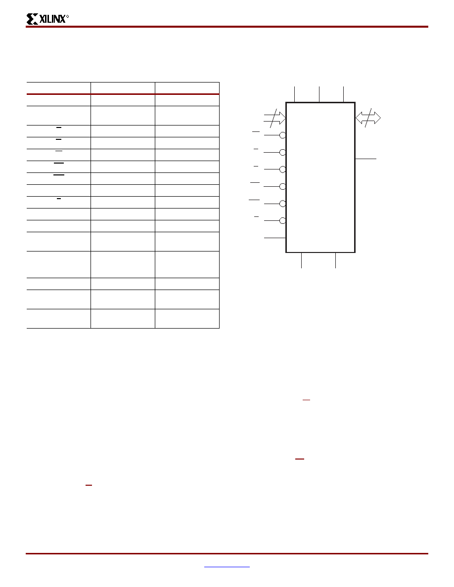
Pinout and Signal Descriptions
See Figure 5 and Table 2 for a logic diagram and brief overview of the signals connected to this device.
Address Inputs (A22-A0)
The Address inputs select the words in the memory array to
access during Bus Read operations. During Bus Write
operations they control the commands sent to the
Command Interface of the Program/Erase Controller.
Data Inputs/Outputs (DQ15-DQ0)
The Data I/O output the data stored at the selected address
during a Bus Read operation or input a command or the
data to be programmed during a Bus Write operation.
Chip Enable (E)
The Chip Enable input activates the memory control logic,
input buffers, decoders and sense amplifiers. When Chip
Enable is at VIL and Reset is at VIH, the device is in active
mode. When Chip Enable is at VIH, the memory is
deselected, the outputs are high impedance, and the power
consumption is reduced to the standby level.
Output Enable (G)
The Output Enable input controls data outputs during the
Bus Read operation of the memory. Before the start of the
first address latching sequence (FALS), the Output Enable
input must be held Low before the clock starts toggling.
Write Enable (W)
The Write Enable input controls the Bus Write operation of
the memory’s Command Interface. The data and address
inputs are latched on the rising edge of Chip Enable or
Write Enable, whichever occurs first.
Table 2: Signal Names
Signal Name
Function
Direction
A22-A0
Address Inputs
Inputs
DQ15-DQ0
Data Input/Outputs,
Command Inputs
I/O
E
Chip Enable
Input
G
Output Enable
Input
W
Write Enable
Input
RP
Reset
Input
WP
Write Protect
Input
K
Clock
Input
L
Latch Enable
Input
READY_WAIT
Ready/Wait
I/O
VDD
Supply Voltage
–
VDDQ
Supply Voltage for
Input/Output Buffers
–
VPP
Optional(1) Supply
Voltage for Fast
Program and Erase
–
VSS
Ground
–
VSSQ
Ground Input/output
Supply
–
NC
Not Connected
Internally
–
Notes:
1.
Typically, VPP is tied to the VDDQ supply on a board. See the VPP
Program Supply Voltage section for alternate options.
X-Ref Target - Figure 5
Figure 5: Logic Diagram
Platform
Flash XL
READY_WAIT
A22–A0
W
K
VSS
VSSQ
VDD
VDDQ
VPP
DQ15–DQ0
16
E
G
RP
WP
L
DS617_05_053008
23
相關(guān)PDF資料 |
PDF描述 |
|---|---|
| XCF32PFS48C | IC PROM SRL 1.8V 32M 48CSBGA |
| XCR3256XL-7CS280C | IC CPLD 256MCELL 3.3V HP 280CSP |
| XCS10-3VQG100C | IC FPGA 5V C-TEMP 100-VQFP |
| XCV600E-8HQ240C | IC FPGA 1.8V C-TEMP 240-HQFP |
| XCV812E-8FG900C | IC FPGA 1.8V C-TEMP 900-FBGA |
相關(guān)代理商/技術(shù)參數(shù) |
參數(shù)描述 |
|---|---|
| XCF128XFTG64CES | 制造商:Xilinx 功能描述: |
| XCF12-L4Z1 | 制造商:SAIA - BURGESS ELECTRONICS INC. 功能描述:Catalogue / XCF12-L4Z1 |
| XCF12-S1 | 制造商:SAIA - BURGESS ELECTRONICS INC. 功能描述:Catalogue / XCF12-S1 |
| XCF13-S1 | 制造商:SAIA - BURGESS ELECTRONICS INC. 功能描述:Catalogue / XCF13-S1 |
| XCF16P | 制造商:XILINX 制造商全稱(chēng):XILINX 功能描述:Platform Flash In-System Programmable Configuration PROMs |
發(fā)布緊急采購(gòu),3分鐘左右您將得到回復(fù)。