- 您現(xiàn)在的位置:買賣IC網(wǎng) > PDF目錄1974 > XCF128XFTG64C (Xilinx Inc)IC PROM SRL 128M GATE 64-FTBGA PDF資料下載
參數(shù)資料
| 型號: | XCF128XFTG64C |
| 廠商: | Xilinx Inc |
| 文件頁數(shù): | 3/88頁 |
| 文件大小: | 0K |
| 描述: | IC PROM SRL 128M GATE 64-FTBGA |
| 標準包裝: | 1 |
| 可編程類型: | 系統(tǒng)內(nèi)可編程 |
| 存儲容量: | 128Mb |
| 電源電壓: | 1.7 V ~ 2 V |
| 工作溫度: | -40°C ~ 85°C |
| 封裝/外殼: | 64-TBGA |
| 供應(yīng)商設(shè)備封裝: | 64-TFBGA |
| 包裝: | 托盤 |
| 產(chǎn)品目錄頁面: | 601 (CN2011-ZH PDF) |
| 其它名稱: | 122-1578 |
第1頁第2頁當(dāng)前第3頁第4頁第5頁第6頁第7頁第8頁第9頁第10頁第11頁第12頁第13頁第14頁第15頁第16頁第17頁第18頁第19頁第20頁第21頁第22頁第23頁第24頁第25頁第26頁第27頁第28頁第29頁第30頁第31頁第32頁第33頁第34頁第35頁第36頁第37頁第38頁第39頁第40頁第41頁第42頁第43頁第44頁第45頁第46頁第47頁第48頁第49頁第50頁第51頁第52頁第53頁第54頁第55頁第56頁第57頁第58頁第59頁第60頁第61頁第62頁第63頁第64頁第65頁第66頁第67頁第68頁第69頁第70頁第71頁第72頁第73頁第74頁第75頁第76頁第77頁第78頁第79頁第80頁第81頁第82頁第83頁第84頁第85頁第86頁第87頁第88頁
Platform Flash XL High-Density Configuration and Storage Device
DS617 (v3.0.1) January 07, 2010
Product Specification
11
R
Bus Operations
There are six standard bus operations that control the
device: Bus Read, Bus Write, Address Latch, Output
Disable, Standby and Reset (Table 5).
Bus Read
Bus Read operations are used to output the contents of the
Memory Array, Electronic Signature, Status Register and
Common Flash Interface. Both Chip Enable and Output
Enable must be at VIL in order to perform a read operation.
The Chip Enable input should be used to enable the device.
Output Enable should be used to gate data onto the output.
The data read depends on the previous command written to
the memory (see “Command Interface,” page 14).
Bus Write
Bus Write operations write commands to the memory or
latch Input Data to be programmed. A Bus Write operation
is initiated when Chip Enable and Write Enable are at VIL
with Output Enable at VIH. Commands, Input Data and
Addresses are latched on the rising edge of Write Enable or
Chip Enable, whichever occurs first. The addresses can be
latched prior to the write operation by toggling Latch Enable
(when Chip Enable is at VIL).
The Latch Enable signal can also be held at VIL by the
system, but then the system must guarantee that the
address lines remain stable for at least TWHAX.
Note: Typically glitches of less than 5 ns on Chip Enable or
Write Enable are ignored by the memory and do not affect Bus
Write operations.
Address Latch
Address latch operations input valid addresses. Both Chip
enable and Latch Enable must be at VIL during address
latch operations. Addresses are latched on the rising edge
of Latch Enable.
Output Disable
The outputs are held at high impedance when Output
Enable is at VIH.
Standby
Standby disables most of the internal circuitry allowing a
substantial reduction of the current consumption. The
memory is in standby when Chip Enable and Reset are at
VIH. Power consumption is reduced to the standby level
IDD3, and the outputs are set to high impedance
independently from Output Enable or Write Enable. If Chip
Enable switches to VIH during a program or erase operation,
the device enters Standby mode when finished with the
program or erase operation.
Reset
During Reset mode, the memory is deselected and the
outputs are high impedance. The memory is in Reset mode
when Reset is at VIL. Power consumption is reduced to the
Reset level independently from Chip Enable, Output Enable
or Write Enable. If Reset is pulled to VSS during a Program
or Erase, this operation is aborted and the memory content
is no longer valid.
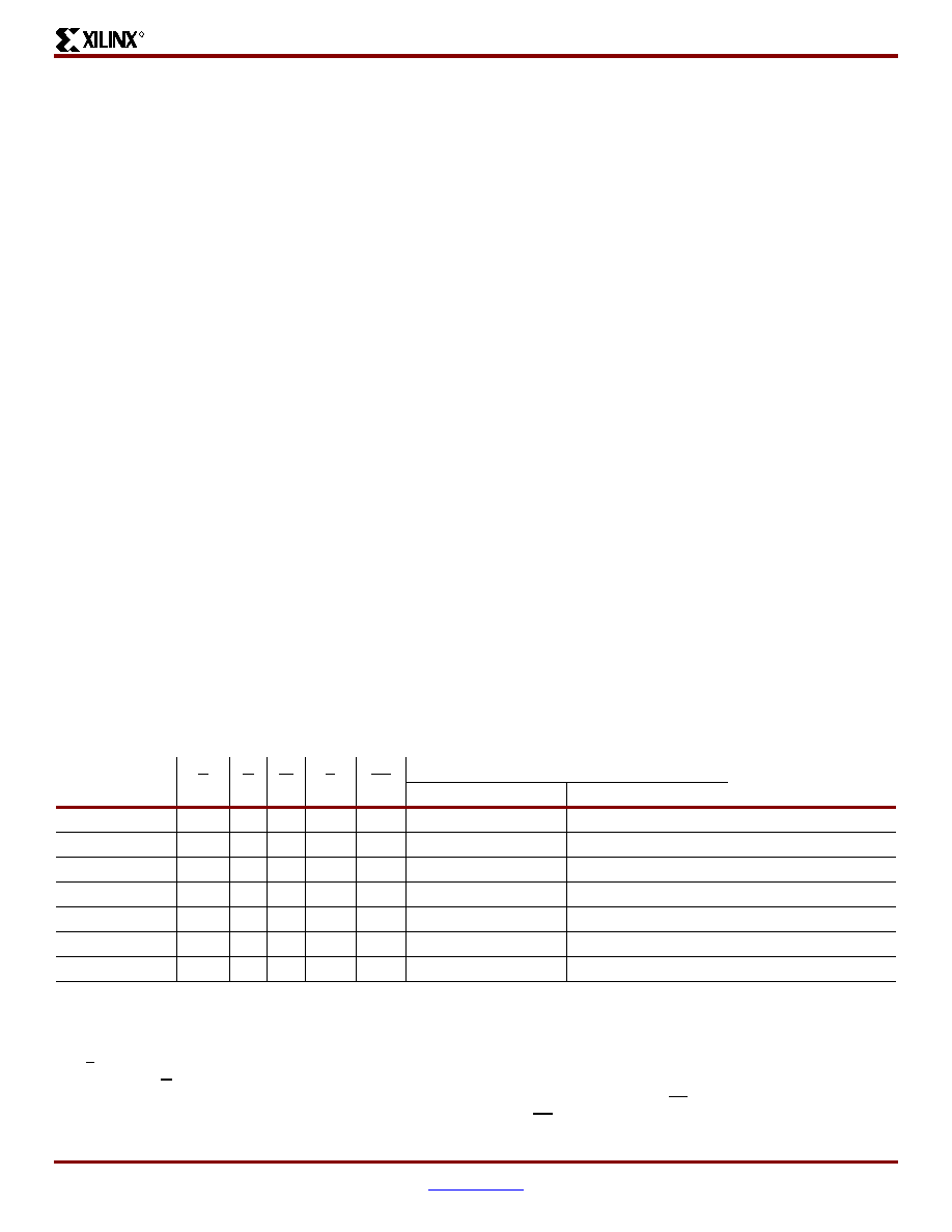
Table 5: Bus Operations(1)
Operation
E
G
W
L
RP
READY_WAIT(2,3)
DQ15-DQ0
CR4 = 1
CR4 = 0
Bus Read
VIL
VIH
VIL(4)
VIH
Hi-Z
–
Data output
Bus Write
VIL
VIH
VIL
VIL(4)
VIH
Hi-Z
–
Data input
Address Latch
VIL
XVIH
VIL
VIH
Hi-Z
–
Data output or Hi-Z(5)
Output Disable
VIL
VIH
XVIH
Hi-Z
Standby
VIH
XX
X
VIH
Hi-Z
Reset
X
VIL(6)
VIL(7)
–
Hi-Z
FALS
VIL
VIH
Hi-Z
–
Data output
Notes:
1.
X = Don't care.
2.
If READY_WAIT is configured as an output wait signal (CR4 = 0), then the CR10 Configuration Register bit defines the signal polarity.
3.
READY_WAIT is configured using the CR4 Configuration Register bit.
4.
L can be tied to VIH if the valid address was previously latched.
5.
Depends on G.
6.
The Configuration Register reverts to its default value after a Low logic level (VIL) is detected on the RP pin.
7.
READY_WAIT pin used as an output. READY_WAIT goes Low TPLRWL after RP goes Low.
相關(guān)PDF資料 |
PDF描述 |
|---|---|
| XCF32PFS48C | IC PROM SRL 1.8V 32M 48CSBGA |
| XCR3256XL-7CS280C | IC CPLD 256MCELL 3.3V HP 280CSP |
| XCS10-3VQG100C | IC FPGA 5V C-TEMP 100-VQFP |
| XCV600E-8HQ240C | IC FPGA 1.8V C-TEMP 240-HQFP |
| XCV812E-8FG900C | IC FPGA 1.8V C-TEMP 900-FBGA |
相關(guān)代理商/技術(shù)參數(shù) |
參數(shù)描述 |
|---|---|
| XCF128XFTG64CES | 制造商:Xilinx 功能描述: |
| XCF12-L4Z1 | 制造商:SAIA - BURGESS ELECTRONICS INC. 功能描述:Catalogue / XCF12-L4Z1 |
| XCF12-S1 | 制造商:SAIA - BURGESS ELECTRONICS INC. 功能描述:Catalogue / XCF12-S1 |
| XCF13-S1 | 制造商:SAIA - BURGESS ELECTRONICS INC. 功能描述:Catalogue / XCF13-S1 |
| XCF16P | 制造商:XILINX 制造商全稱:XILINX 功能描述:Platform Flash In-System Programmable Configuration PROMs |
發(fā)布緊急采購,3分鐘左右您將得到回復(fù)。