- 您現(xiàn)在的位置:買賣IC網(wǎng) > PDF目錄98068 > S1C60N08F0A0100 MICROCONTROLLER, PQFP100 PDF資料下載
參數(shù)資料
| 型號(hào): | S1C60N08F0A0100 |
| 元件分類: | 微控制器/微處理器 |
| 英文描述: | MICROCONTROLLER, PQFP100 |
| 封裝: | PLASTIC, QFP-100 |
| 文件頁數(shù): | 88/145頁 |
| 文件大?。?/td> | 1118K |
| 代理商: | S1C60N08F0A0100 |
第1頁第2頁第3頁第4頁第5頁第6頁第7頁第8頁第9頁第10頁第11頁第12頁第13頁第14頁第15頁第16頁第17頁第18頁第19頁第20頁第21頁第22頁第23頁第24頁第25頁第26頁第27頁第28頁第29頁第30頁第31頁第32頁第33頁第34頁第35頁第36頁第37頁第38頁第39頁第40頁第41頁第42頁第43頁第44頁第45頁第46頁第47頁第48頁第49頁第50頁第51頁第52頁第53頁第54頁第55頁第56頁第57頁第58頁第59頁第60頁第61頁第62頁第63頁第64頁第65頁第66頁第67頁第68頁第69頁第70頁第71頁第72頁第73頁第74頁第75頁第76頁第77頁第78頁第79頁第80頁第81頁第82頁第83頁第84頁第85頁第86頁第87頁當(dāng)前第88頁第89頁第90頁第91頁第92頁第93頁第94頁第95頁第96頁第97頁第98頁第99頁第100頁第101頁第102頁第103頁第104頁第105頁第106頁第107頁第108頁第109頁第110頁第111頁第112頁第113頁第114頁第115頁第116頁第117頁第118頁第119頁第120頁第121頁第122頁第123頁第124頁第125頁第126頁第127頁第128頁第129頁第130頁第131頁第132頁第133頁第134頁第135頁第136頁第137頁第138頁第139頁第140頁第141頁第142頁第143頁第144頁第145頁
S1C60N08 TECHNICAL HARDWARE
EPSON
I-35
CHAPTER 4: PERIPHERAL CIRCUITS AND OPERATION (Serial Interface)
Note: When using the serial interface in the master mode, CPU system clock is used as the synchronous
clock. Accordingly, when the serial interface is operating, system clock switching (fOSC1
fOSC3)
should not be performed.
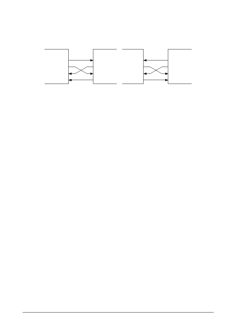
A sample basic serial input/output portion connection is shown in Figure 4.7.2.1.
S1C60N08
Master mode
Slave mode
SCLK
SOUT
SIN
Input terminal
External
serial device
CLK
SOUT
SIN
READY
S1C60N08
SCLK
SOUT
SIN
R11(SIOF)
External
serial device
CLK
SOUT
SIN
Input terminal
Fig. 4.7.2.1 Sample basic connection
4.7.3 Data input/output and interrupt function
The serial interface can input/output data via the internal 8 bits shift register. The shift register operates
by synchronizing with either the synchronous clock output from SCLK terminal (master mode), or the
synchronous clock input to SCLK (slave mode).
The serial interface generates interrupt on completion of the 8 bits serial data input/output. Detection of
serial data input/output is done by the counting of the synchronous clock (SCLK); the clock completes
input/output operation when 8 counts (equivalent to 8 cycles) have been made and then generates
interrupt.
The serial data input/output procedure data is explained below:
(1) Serial data output procedure and interrupt
The serial interface is capable of outputting parallel data as serial data, in units of 8 bits.
By setting the parallel data to 4 bits registers SD0–SD3 (address 2F0H) and SD4–SD7 (address 2F1H)
individually and writing "1" to SCTRG bit (address 2E7HD3), it synchronizes with the synchronous
clock and serial data is output at the SOUT terminal. The synchronous clock used here is as follows: in
the master mode, internal clock which is output to the SCLK terminal while in the slave mode,
external clock which is input from the SCLK terminal. The serial output of the SOUT termina changes
with the rising edge of the clock that is input or output from the SCLK terminal.
The serial data to the built-in shift register is shifted with the rising edge of the SCLK signal when SE2
bit (address 2F2HD1) is "1" and is shifted with the falling edge of the SCLK signal when SE2 bit
(address 2F2HD1) is "0".
When the output of the 8 bits data from SD0 to SD7 is completed, the interrupt factor flag ISIO
(address 2F3HD0) is set to "1" and interrupt is generated. Moreover, the interrupt can be masked by
the interrupt mask register EISIO (address 2F2HD0).
(2) Serial data input procedure and interrupt
The serial interface is capable of inputting serial data as parallel data, in units of 8 bits.
The serial data is input from the SIN terminal, synchronizes with the synchronous clock, and is
sequentially read in the 8 bits shift register. As in the above item (1), the synchronous clock used here
is as follows: in the master mode, internal clock which is output to the SCLK terminal while in the
slave mode, external clock which is input from the SCLK terminal.
The serial data to the built-in shift register is read with the rising edge of the SCLK signal when SE2
bit is "1" and is read with the falling edge of the SCLK signal when SE2 bit is "0". Moreover, the shift
register is sequentially shifted as the data is fetched.
When the input of the 8 bits data from SD0 to SD7 is completed, the interrupt factor flag ISIO is set to
"1" and interrupt is generated. Moreover, the interrupt can be masked by the interrupt mask register
EISIO. Note, however, that regardless of the setting of the interrupt mask register, the interrupt factor
flag is set to "1" after input of the 8 bits data.
The data input in the shift register can be read from data registers SD0–SD7 by software.
相關(guān)PDF資料 |
PDF描述 |
|---|---|
| S1C621C0D | 4-BIT, MROM, 1.3 MHz, MICROCONTROLLER, UUC74 |
| S1C62480D | 4-BIT, MROM, 2.3 MHz, MICROCONTROLLER, UUC135 |
| S1C62440F | 4-BIT, MROM, 2.3 MHz, MICROCONTROLLER, PQFP128 |
| S1C62740D | 4-BIT, MROM, 1.3 MHz, MICROCONTROLLER, UUC109 |
| S1C62920D | 4-BIT, MROM, 1.3 MHz, MICROCONTROLLER, UUC63 |
相關(guān)代理商/技術(shù)參數(shù) |
參數(shù)描述 |
|---|---|
| S1C60N16 | 制造商:EPSON 制造商全稱:EPSON 功能描述:4-bit Single Chip Microcomputer |
| S1C60R08 | 制造商:EPSON 制造商全稱:EPSON 功能描述:4-bit Single Chip Microcomputer |
| S1C63004 | 制造商:EPSON 制造商全稱:EPSON 功能描述:CMOS 4-bit Single Chip Microcontroller |
| S1C63008 | 制造商:EPSON 制造商全稱:EPSON 功能描述:CMOS 4-bit Single Chip Microcontroller |
| S1C63016 | 制造商:EPSON 制造商全稱:EPSON 功能描述:CMOS 4-bit Single Chip Microcontroller |
發(fā)布緊急采購,3分鐘左右您將得到回復(fù)。