- 您現(xiàn)在的位置:買賣IC網(wǎng) > PDF目錄98068 > S1C60N08F0A0100 MICROCONTROLLER, PQFP100 PDF資料下載
參數(shù)資料
| 型號: | S1C60N08F0A0100 |
| 元件分類: | 微控制器/微處理器 |
| 英文描述: | MICROCONTROLLER, PQFP100 |
| 封裝: | PLASTIC, QFP-100 |
| 文件頁數(shù): | 63/145頁 |
| 文件大小: | 1118K |
| 代理商: | S1C60N08F0A0100 |
第1頁第2頁第3頁第4頁第5頁第6頁第7頁第8頁第9頁第10頁第11頁第12頁第13頁第14頁第15頁第16頁第17頁第18頁第19頁第20頁第21頁第22頁第23頁第24頁第25頁第26頁第27頁第28頁第29頁第30頁第31頁第32頁第33頁第34頁第35頁第36頁第37頁第38頁第39頁第40頁第41頁第42頁第43頁第44頁第45頁第46頁第47頁第48頁第49頁第50頁第51頁第52頁第53頁第54頁第55頁第56頁第57頁第58頁第59頁第60頁第61頁第62頁當(dāng)前第63頁第64頁第65頁第66頁第67頁第68頁第69頁第70頁第71頁第72頁第73頁第74頁第75頁第76頁第77頁第78頁第79頁第80頁第81頁第82頁第83頁第84頁第85頁第86頁第87頁第88頁第89頁第90頁第91頁第92頁第93頁第94頁第95頁第96頁第97頁第98頁第99頁第100頁第101頁第102頁第103頁第104頁第105頁第106頁第107頁第108頁第109頁第110頁第111頁第112頁第113頁第114頁第115頁第116頁第117頁第118頁第119頁第120頁第121頁第122頁第123頁第124頁第125頁第126頁第127頁第128頁第129頁第130頁第131頁第132頁第133頁第134頁第135頁第136頁第137頁第138頁第139頁第140頁第141頁第142頁第143頁第144頁第145頁
I-12
EPSON
S1C60N08 TECHNICAL HARDWARE
CHAPTER 4: PERIPHERAL CIRCUITS AND OPERATION (Memory Map)
CHAPTER
4PERIPHERAL CIRCUITS AND OPERATION
Peripheral circuits (timer, I/O, and so on) of the S1C60N08 Series are memory mapped. Thus, all the
peripheral circuits can be controlled by using memory operations to access the I/O memory. The follow-
ing sections describe how the peripheral circuits operate.
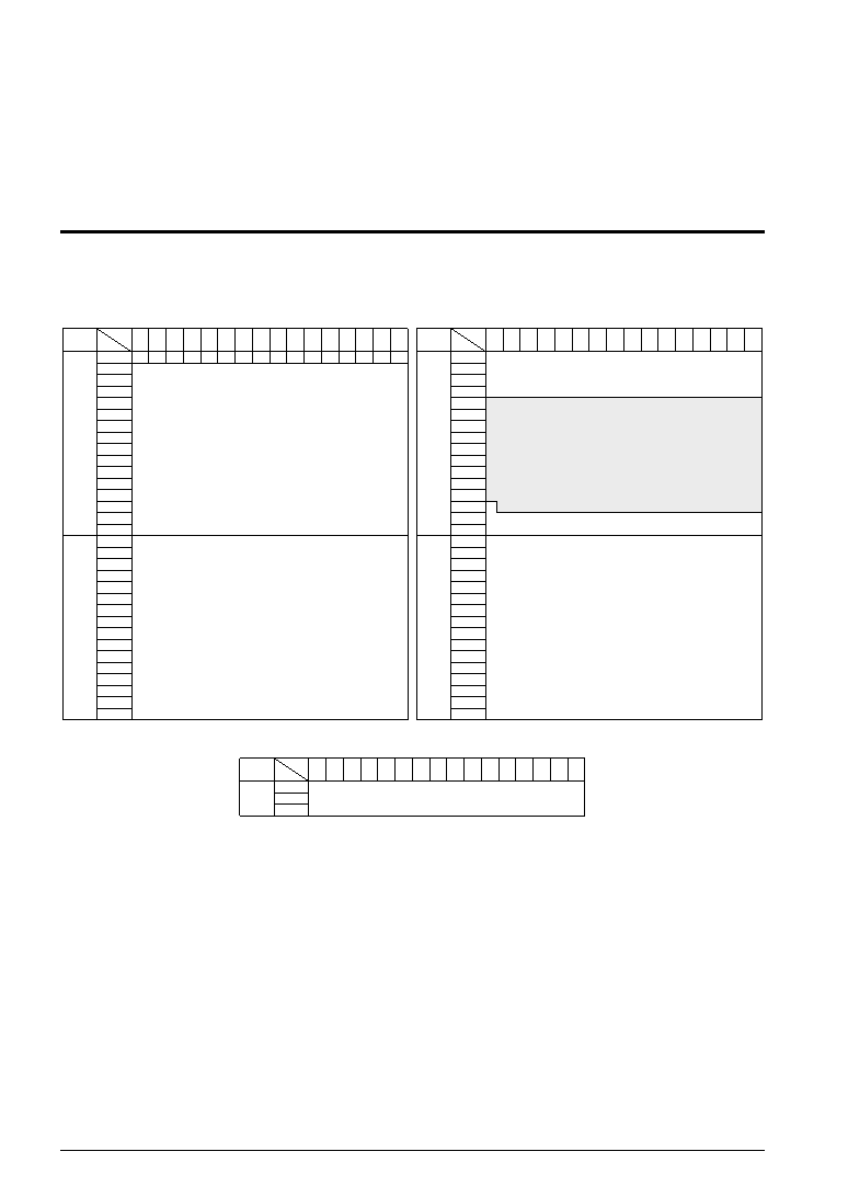
4.1 Memory Map
The data memory of the S1C60N08 Series has an address space of 865 words (913 words when display
memory is laid out in Page 2), of which 48 words are allocated to display memory and 33 words, to I/O
memory. Figure 4.1.1 shows the overall memory map for the S1C60N08 Series, and Tables 4.1.1(a)–(c), the
memory maps for the peripheral circuits (I/O space).
2
0
1
2
3
4
5
6
7
8
9
A
B
C
D
E
F
Address
Page
Low
High
0
1
2
3
4
5
6
7
8
9
A
B
C
D
E
F
M0 M1 M2 M3 M4 M5 M6 M7 M8 M9 MA MB MC MD ME MF
0
1
2
3
4
5
6
7
8
9
A
B
C
D
E
F
RAM (256 words
× 4 bits)
R/W
1
0
1
2
3
4
5
6
7
8
9
A
B
C
D
E
F
RAM (256 words
× 4 bits)
R/W
Address
Page
Low
High
0
1
2
3
4
5
6
7
8
9
A
B
C
D
E
F
RAM (64 words
× 4 bits)
R/W
I/O mamory (see Table 4.1.1)
Unused area
3
0
1
2
3
4
5
6
7
8
9
A
B
C
D
E
F
RAM (256 words
× 4 bits)
R/W
Fig. 4.1.1 Memory map
Address
Page
Low
High
0
1
2
3
4
5
6
7
8
9
A
B
C
D
E
F
0 or 2
4
5
6
Display memory (48 words
× 4 bits)
Page 0: R/W, Page 2: W only
Fig. 4.1.2 Display memory map
Notes: The display memory area can be selected from between Page 0 (040H–06FH) and Page 2
(240H–26FH) by mask option.
When Page 0 (040H–06FH) is selected, the display memory is assigned in the RAM area. So
read/write operation is allowed.
When Page 2 (240H–26FH) is selected, the display memory is assigned as a write-only memory.
Memory is not mounted in unused area within the memory map and in memory area not indi-
cated in this chapter. For this reason, normal operation cannot be assured for programs that
have been prepared with access to these areas.
相關(guān)PDF資料 |
PDF描述 |
|---|---|
| S1C621C0D | 4-BIT, MROM, 1.3 MHz, MICROCONTROLLER, UUC74 |
| S1C62480D | 4-BIT, MROM, 2.3 MHz, MICROCONTROLLER, UUC135 |
| S1C62440F | 4-BIT, MROM, 2.3 MHz, MICROCONTROLLER, PQFP128 |
| S1C62740D | 4-BIT, MROM, 1.3 MHz, MICROCONTROLLER, UUC109 |
| S1C62920D | 4-BIT, MROM, 1.3 MHz, MICROCONTROLLER, UUC63 |
相關(guān)代理商/技術(shù)參數(shù) |
參數(shù)描述 |
|---|---|
| S1C60N16 | 制造商:EPSON 制造商全稱:EPSON 功能描述:4-bit Single Chip Microcomputer |
| S1C60R08 | 制造商:EPSON 制造商全稱:EPSON 功能描述:4-bit Single Chip Microcomputer |
| S1C63004 | 制造商:EPSON 制造商全稱:EPSON 功能描述:CMOS 4-bit Single Chip Microcontroller |
| S1C63008 | 制造商:EPSON 制造商全稱:EPSON 功能描述:CMOS 4-bit Single Chip Microcontroller |
| S1C63016 | 制造商:EPSON 制造商全稱:EPSON 功能描述:CMOS 4-bit Single Chip Microcontroller |
發(fā)布緊急采購,3分鐘左右您將得到回復(fù)。