- 您現(xiàn)在的位置:買賣IC網(wǎng) > PDF目錄359234 > MT90520AG (ZARLINK SEMICONDUCTOR INC) 8-Port Primary Rate Circuit Emulation AAL1 SAR PDF資料下載
參數(shù)資料
| 型號(hào): | MT90520AG |
| 廠商: | ZARLINK SEMICONDUCTOR INC |
| 元件分類: | 數(shù)字傳輸電路 |
| 英文描述: | 8-Port Primary Rate Circuit Emulation AAL1 SAR |
| 中文描述: | ATM SEGMENTATION AND REASSEMBLY DEVICE, PBGA456 |
| 封裝: | 35 X 35 MM, 1.27 MM PITCH, PLASTIC, MS-034, BGA-456 |
| 文件頁數(shù): | 60/180頁 |
| 文件大小: | 1736K |
| 代理商: | MT90520AG |
第1頁第2頁第3頁第4頁第5頁第6頁第7頁第8頁第9頁第10頁第11頁第12頁第13頁第14頁第15頁第16頁第17頁第18頁第19頁第20頁第21頁第22頁第23頁第24頁第25頁第26頁第27頁第28頁第29頁第30頁第31頁第32頁第33頁第34頁第35頁第36頁第37頁第38頁第39頁第40頁第41頁第42頁第43頁第44頁第45頁第46頁第47頁第48頁第49頁第50頁第51頁第52頁第53頁第54頁第55頁第56頁第57頁第58頁第59頁當(dāng)前第60頁第61頁第62頁第63頁第64頁第65頁第66頁第67頁第68頁第69頁第70頁第71頁第72頁第73頁第74頁第75頁第76頁第77頁第78頁第79頁第80頁第81頁第82頁第83頁第84頁第85頁第86頁第87頁第88頁第89頁第90頁第91頁第92頁第93頁第94頁第95頁第96頁第97頁第98頁第99頁第100頁第101頁第102頁第103頁第104頁第105頁第106頁第107頁第108頁第109頁第110頁第111頁第112頁第113頁第114頁第115頁第116頁第117頁第118頁第119頁第120頁第121頁第122頁第123頁第124頁第125頁第126頁第127頁第128頁第129頁第130頁第131頁第132頁第133頁第134頁第135頁第136頁第137頁第138頁第139頁第140頁第141頁第142頁第143頁第144頁第145頁第146頁第147頁第148頁第149頁第150頁第151頁第152頁第153頁第154頁第155頁第156頁第157頁第158頁第159頁第160頁第161頁第162頁第163頁第164頁第165頁第166頁第167頁第168頁第169頁第170頁第171頁第172頁第173頁第174頁第175頁第176頁第177頁第178頁第179頁第180頁
MT90520
Data Sheet
60
Zarlink Semiconductor Inc.
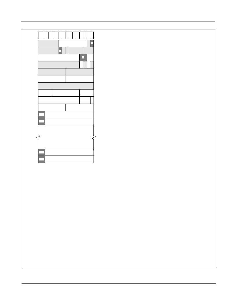
Figure 22 - Segmentation Control Structure - SDT Format
Note 1:
Fields which appear in dark grey are reserved fields
which must be cleared by software upon initialization.
Note 2
: Fields which appear in light grey are those which are
updated by hardware.
Number of TDM Octets:
Indicates the number of TDM octets required to fill the next
cell of the corresponding VC. Initialize to 47d.
Number of Channels:
Indicates the number of TDM channels in the VC associated
with this control structure (possible values = 1d to 128d).
RM (Remainder):
When set, this bit indicates that there is enough TDM data to create
more than one cell in the current frame. Initialize to ‘0’.
Read Pointer:
This value represents the location in the circular buffers from which the
next TDM value will be read. Should generally be initialized to “0”, but if the chip is sup-
porting a large number of VCs, this field may be used to distribute cell generation over
more than 1 frame. See “Read Pointer Field” on page 61 for more details.
W (Wait for Multiframe):
When set, the TX_SAR module waits for the multiframe
boundary to produce the first cell (seq. num = 0; pointer = 0).
F (First Cell):
If set, indicates that the next cell is the first one to be sent for the current
VC. Should be initialized to ‘1’, except if the
Read Pointer
is used to scatter the cell
generation over multiple frames (this bit should then be cleared).
SRTS:
If
SE
is set, an SRTS value is read from the Clock Management module at the
beginning of each cell sequence (SN = 0) and stored in this field. In cells with odd
sequence numbers, the MSB from this field is placed into the CSI bit of the SAR-PDU
header. The
SRTS
value is then shifted left.
SN (Sequence Number):
Holds the sequence number of the next cell to be gener-
ated. Must be initialized to “0”.
Structure Length:
This field contains the length of the multiframe structure (payload
substructure + signalling substructure). For non-CAS VCs, this field should be initial-
ized to
Number of Channels
. For CAS VCs, this field = (
Number of Channels
)*m +
roundup(
Number of Channels
/2) where m=24 for DS1 and 16 for E1.
M (Mode):
“01” = (DS1 with CAS and
Number of Channels
= 1); “10” = (E1 with CAS
and
Number of Channels
= 1); “11” = (E1 with CAS and
Number of Channels
= 2);
“00” = all other cases.
Structure Boundary Pointer:
Indicates the distance, in octets, between the last pay-
load byte written and the next structure boundary. Initialize to “0”.
SE (SRTS Enable):
When set, indicates that the VC is transmitting SRTS data. When
cleared, the CSI bit of outgoing odd-numbered cells is set to ‘0’. Only one VC per port
may carry SRTS information.
PS (Pointer Sent):
Used to ensure that only a single pointer cell is sent within an
eight-cell sequence. Initialize to ‘0’.
PE (Pointer Enable):
When set, a pointer cell will be generated once per 8-cell
sequence. This bit must be cleared to ‘0’ for single-channel VCs not transporting CAS,
but set in all other cases.
P (Pointer Cell):
Indicates that the next cell to be produced will be a pointer cell.
Should be initialized to the same value as the
PE
bit.
Current CAS:
When transporting CAS, this field is used to keep track of which circular
buffer pointer to read next. Must be initialized to 0Ah.
Current TDM:
Used to keep track of which circular buffer pointer to read next. Must be
initialized to 0Ah.
Last:
Contains the address (relative to word 0) of the last valid
Segmentation Circu-
lar Buffer Base Address
in the control structure. The formula for this field is: 09h
+
Number of Channels
.
Number of CAS:
Contains the size, in octets, of the signalling substructure. If CAS is
not being transmitted, this field should be initialized to “0”. Otherwise, the formula is:
roundup(
Number of Channels
/2).
Cell Count Statistic:
Rollover counter which counts the number of cells transmitted
on this VC by the TX_SAR module. Initialize to “0”.
GFC:
The Generic Flow Control value is placed in the GFC field of cell headers in a
UNI cell. If the cell is using NNI formatting, these bits hold the four MSBs of the VPI.
VPI:
This value is placed in the VPI field of outgoing cell headers.
VCI:
This value is placed in the VCI field of the generated cell headers.
PTI:
This value is placed in the PTI field of outgoing cell headers.
C (CLP):
This value is placed in the CLP field of the cell headers.
HEC:
This value is placed in the HEC (UDF1) field of outgoing cell headers. The phys-
ical layer is generally responsible for calculating HEC values; therefore, this field is
used as a place holder. If the physical layer does not calculate the HEC, the user may
generate the appropriate HEC value by performing a modulo-2 division of the first four
octets of the cell header using the generator polynomial G(x) = x
8
+ x
2
+ x + 1.
UDF2:
This value is placed in the UDF2 field of the cell header when the UTOPIA is
operating in 16-bit mode.
Segmentation Circular Buffer X Base Address:
The bits of this field are concate-
nated with the
Read Pointer
bits to form a 20-bit
word
address to external memory.
This value is used to address a particular TDM or CAS value in a particular buffer. One
pointer is needed for each channel in the VC.
0
15
1
2
3
4
5
6
7
8
9
10
11
12
13
14
Number of
TDM Octets
Read
Pointer
Number of
Channels
R
R W F
SRTS
SN
Structure Length
R
M
Current CAS
Current TDM
Last
Number of CAS
Cell Count Statistic
GFC
VPI
VCI
VCI
PTI
C
HEC
UDF2
Segmentation Circular Buffer 0
Base Address (bits<19:6>)
Segmentation Circular Buffer 1
Base Address (bits<19:6>)
Segmentation Circular Buffer 126
Base Address (bits<19:6>)
Segmentation Circular Buffer 127
Base Address (bits<19:6>)
Minimum Structure Size -
22 bytes (1 channel)
Maximum Structure Size -
276 bytes (128 channels)
+00
Byte
Add
+02
+04
+08
+06
+0A
+0C
+0E
+12
+10
+16
+14
+112
+110
+00
Word
Add
+01
+02
+03
+04
+05
+06
+07
+08
+09
+0A
+0B
+88
+89
Res
Res
Res
Res
Structure Boundary Pointer
S
E
P
S
P
相關(guān)PDF資料 |
PDF描述 |
|---|---|
| MT9072 | Ultraframer DS3/E3/DS2/E2/DS1/E1/DS0 |
| MT9072AB | Ultraframer DS3/E3/DS2/E2/DS1/E1/DS0 |
| MT9072AV | Ultraframer DS3/E3/DS2/E2/DS1/E1/DS0 |
| MT90820 | Large Digital Switch |
| MT90820AL | Large Digital Switch |
相關(guān)代理商/技術(shù)參數(shù) |
參數(shù)描述 |
|---|---|
| MT90520AG2 | 制造商:Microsemi Corporation 功能描述:ATM SAR 2.048MBPS 2.5V CBR 456BGA - Trays 制造商:Zarlink Semiconductor Inc 功能描述:ATM SAR 2.048MBPS 2.5V CBR 456BGA - Trays |
| MT90528 | 制造商:ZARLINK 制造商全稱:Zarlink Semiconductor Inc 功能描述:28-Port Primary Rate Circuit Emulation AAL1 SAR |
| MT90528AG | 制造商:ZARLINK 制造商全稱:Zarlink Semiconductor Inc 功能描述:28-Port Primary Rate Circuit Emulation AAL1 SAR |
| MT90528AG2 | 制造商:ZARLINK 制造商全稱:Zarlink Semiconductor Inc 功能描述:28-Port Primary Rate Circuit Emulation AAL1 SAR |
| MT90710 | 制造商:MITEL 制造商全稱:Mitel Networks Corporation 功能描述:High-Speed Isochronous Multiplexer |
發(fā)布緊急采購,3分鐘左右您將得到回復(fù)。