- 您現(xiàn)在的位置:買賣IC網(wǎng) > PDF目錄359234 > MT90520AG (ZARLINK SEMICONDUCTOR INC) 8-Port Primary Rate Circuit Emulation AAL1 SAR PDF資料下載
參數(shù)資料
| 型號: | MT90520AG |
| 廠商: | ZARLINK SEMICONDUCTOR INC |
| 元件分類: | 數(shù)字傳輸電路 |
| 英文描述: | 8-Port Primary Rate Circuit Emulation AAL1 SAR |
| 中文描述: | ATM SEGMENTATION AND REASSEMBLY DEVICE, PBGA456 |
| 封裝: | 35 X 35 MM, 1.27 MM PITCH, PLASTIC, MS-034, BGA-456 |
| 文件頁數(shù): | 19/180頁 |
| 文件大小: | 1736K |
| 代理商: | MT90520AG |
第1頁第2頁第3頁第4頁第5頁第6頁第7頁第8頁第9頁第10頁第11頁第12頁第13頁第14頁第15頁第16頁第17頁第18頁當(dāng)前第19頁第20頁第21頁第22頁第23頁第24頁第25頁第26頁第27頁第28頁第29頁第30頁第31頁第32頁第33頁第34頁第35頁第36頁第37頁第38頁第39頁第40頁第41頁第42頁第43頁第44頁第45頁第46頁第47頁第48頁第49頁第50頁第51頁第52頁第53頁第54頁第55頁第56頁第57頁第58頁第59頁第60頁第61頁第62頁第63頁第64頁第65頁第66頁第67頁第68頁第69頁第70頁第71頁第72頁第73頁第74頁第75頁第76頁第77頁第78頁第79頁第80頁第81頁第82頁第83頁第84頁第85頁第86頁第87頁第88頁第89頁第90頁第91頁第92頁第93頁第94頁第95頁第96頁第97頁第98頁第99頁第100頁第101頁第102頁第103頁第104頁第105頁第106頁第107頁第108頁第109頁第110頁第111頁第112頁第113頁第114頁第115頁第116頁第117頁第118頁第119頁第120頁第121頁第122頁第123頁第124頁第125頁第126頁第127頁第128頁第129頁第130頁第131頁第132頁第133頁第134頁第135頁第136頁第137頁第138頁第139頁第140頁第141頁第142頁第143頁第144頁第145頁第146頁第147頁第148頁第149頁第150頁第151頁第152頁第153頁第154頁第155頁第156頁第157頁第158頁第159頁第160頁第161頁第162頁第163頁第164頁第165頁第166頁第167頁第168頁第169頁第170頁第171頁第172頁第173頁第174頁第175頁第176頁第177頁第178頁第179頁第180頁
MT90520
Data Sheet
19
Zarlink Semiconductor Inc.
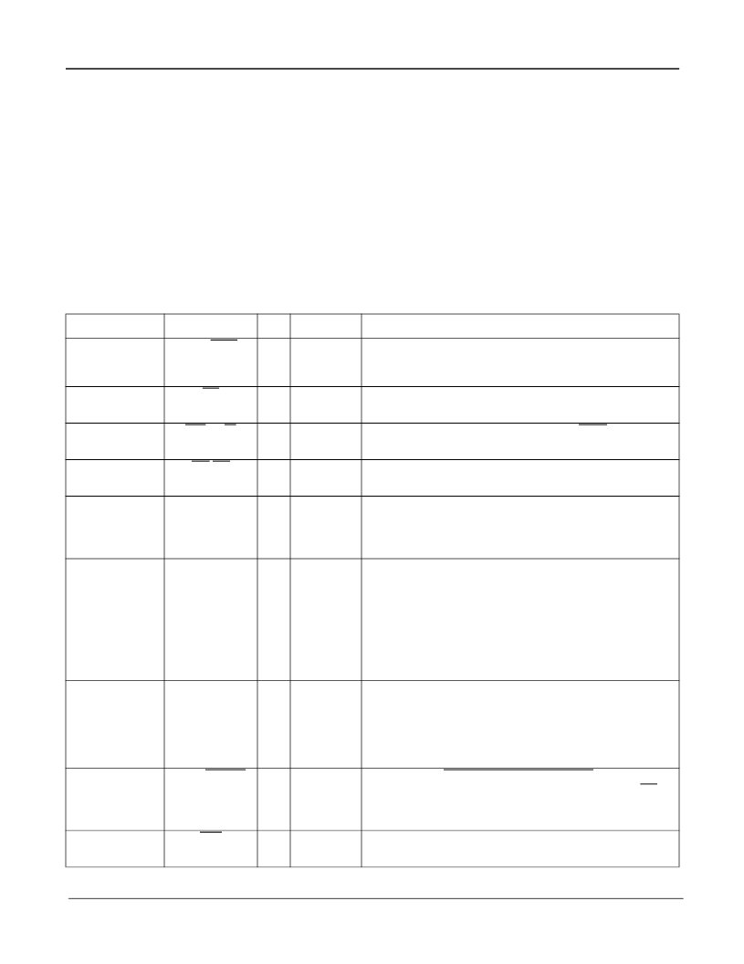
3.0 Pin Descriptions
3.1 Functional Pin Descriptions
Ball pin numbers are given in the following tables as defined in Figure 3.2.3 on page 34. Pins for buses are listed
with the MSB appearing first.
I/O definitions are: Output (O), Input (I), Bidirectional (I/O), Power (PWR), or Ground (GND).
Input pad types are: CMOS or Schmitt, 3.3 V. The notations “PU” and “PD” are used, respectively, to indicate that a
pad has a weak internal pullup or pulldown resistor. All 3.3 V inputs are 5 V tolerant. The 3.3 V CMOS inputs have
a switching threshold of 1.6 V, and tolerate input levels of up to 5 V; therefore they are 5 V TTL compatible.
Output pad types are described by voltage rail and current capability. 3.3 V CMOS outputs will satisfy 5 V TTL input
thresholds at the rated current of the output.
Ball Pin #
Pin Name
I/O
Type
Description
E9
Intel/Moto
I
3.3 V
CMOS PD
This input selects the microprocessor interface mode as
Intel (pulled HIGH) or Motorola (pulled LOW). This pin
must be configured before power-up.
Active LOW chip select signal.
A7
CS
I
3.3 V
CMOS PU
3.3 V
CMOS PU
3.3 V
CMOS PU
3.3 V
CMOS PD
D8
WR/R_W
I
Active LOW Write Strobe (Intel) / Read_Write (Motorola).
C7
RD/DS
I
Active LOW Read Strobe (Intel) / Active LOW Data Strobe
(Motorola).
B7
AEM
I
Access External Memory - CPU accesses external
memory when HIGH (internal memory and registers when
LOW). This pin is usually connected to a high-order CPU
address line.
CPU Address lines A20-A1.
All microprocessor accesses to the device are word-wide,
but addresses in this document are given as byte
addresses. The virtual A[0] bit would select between high
and low bytes within a word.
C15, A16, E15,
D15, B16, C16,
A17, B17, D16,
C17, A18, B18,
C18, D17, A19,
B19, C19, D18,
A20, E17
D9, C8, B8, A8,
D10, C9, B9, A9,
D11, E11, C10,
B10, A10, C11,
B11, D12
C12
CPU_ADD[20:1
]
I
3.3 V
CMOS PD
CPU_DATA[15:
0]
I/O
3.3 V
CMOS PD /
12 mA
CPU data bus. All CPU accesses are word accesses.
RDY/DTACK
O
3.3 V,
24 mA
Ready (Intel) / Data Transfer Acknowledge (Motorola).
Acts as normal output in Intel mode, tristated when CS is
HIGH; acts as active LOW pseudo-open-drain output in
Motorola mode.
Active LOW interrupt line (operates as open-drain: high-
impedance when inactive).
A11
IRQ
O
3.3 V,
24 mA
Table 1 - Microprocessor Interface Pins
相關(guān)PDF資料 |
PDF描述 |
|---|---|
| MT9072 | Ultraframer DS3/E3/DS2/E2/DS1/E1/DS0 |
| MT9072AB | Ultraframer DS3/E3/DS2/E2/DS1/E1/DS0 |
| MT9072AV | Ultraframer DS3/E3/DS2/E2/DS1/E1/DS0 |
| MT90820 | Large Digital Switch |
| MT90820AL | Large Digital Switch |
相關(guān)代理商/技術(shù)參數(shù) |
參數(shù)描述 |
|---|---|
| MT90520AG2 | 制造商:Microsemi Corporation 功能描述:ATM SAR 2.048MBPS 2.5V CBR 456BGA - Trays 制造商:Zarlink Semiconductor Inc 功能描述:ATM SAR 2.048MBPS 2.5V CBR 456BGA - Trays |
| MT90528 | 制造商:ZARLINK 制造商全稱:Zarlink Semiconductor Inc 功能描述:28-Port Primary Rate Circuit Emulation AAL1 SAR |
| MT90528AG | 制造商:ZARLINK 制造商全稱:Zarlink Semiconductor Inc 功能描述:28-Port Primary Rate Circuit Emulation AAL1 SAR |
| MT90528AG2 | 制造商:ZARLINK 制造商全稱:Zarlink Semiconductor Inc 功能描述:28-Port Primary Rate Circuit Emulation AAL1 SAR |
| MT90710 | 制造商:MITEL 制造商全稱:Mitel Networks Corporation 功能描述:High-Speed Isochronous Multiplexer |
發(fā)布緊急采購,3分鐘左右您將得到回復(fù)。