- 您現在的位置:買賣IC網 > PDF目錄359234 > MT90520AG (ZARLINK SEMICONDUCTOR INC) 8-Port Primary Rate Circuit Emulation AAL1 SAR PDF資料下載
參數資料
| 型號: | MT90520AG |
| 廠商: | ZARLINK SEMICONDUCTOR INC |
| 元件分類: | 數字傳輸電路 |
| 英文描述: | 8-Port Primary Rate Circuit Emulation AAL1 SAR |
| 中文描述: | ATM SEGMENTATION AND REASSEMBLY DEVICE, PBGA456 |
| 封裝: | 35 X 35 MM, 1.27 MM PITCH, PLASTIC, MS-034, BGA-456 |
| 文件頁數: | 104/180頁 |
| 文件大?。?/td> | 1736K |
| 代理商: | MT90520AG |
第1頁第2頁第3頁第4頁第5頁第6頁第7頁第8頁第9頁第10頁第11頁第12頁第13頁第14頁第15頁第16頁第17頁第18頁第19頁第20頁第21頁第22頁第23頁第24頁第25頁第26頁第27頁第28頁第29頁第30頁第31頁第32頁第33頁第34頁第35頁第36頁第37頁第38頁第39頁第40頁第41頁第42頁第43頁第44頁第45頁第46頁第47頁第48頁第49頁第50頁第51頁第52頁第53頁第54頁第55頁第56頁第57頁第58頁第59頁第60頁第61頁第62頁第63頁第64頁第65頁第66頁第67頁第68頁第69頁第70頁第71頁第72頁第73頁第74頁第75頁第76頁第77頁第78頁第79頁第80頁第81頁第82頁第83頁第84頁第85頁第86頁第87頁第88頁第89頁第90頁第91頁第92頁第93頁第94頁第95頁第96頁第97頁第98頁第99頁第100頁第101頁第102頁第103頁當前第104頁第105頁第106頁第107頁第108頁第109頁第110頁第111頁第112頁第113頁第114頁第115頁第116頁第117頁第118頁第119頁第120頁第121頁第122頁第123頁第124頁第125頁第126頁第127頁第128頁第129頁第130頁第131頁第132頁第133頁第134頁第135頁第136頁第137頁第138頁第139頁第140頁第141頁第142頁第143頁第144頁第145頁第146頁第147頁第148頁第149頁第150頁第151頁第152頁第153頁第154頁第155頁第156頁第157頁第158頁第159頁第160頁第161頁第162頁第163頁第164頁第165頁第166頁第167頁第168頁第169頁第170頁第171頁第172頁第173頁第174頁第175頁第176頁第177頁第178頁第179頁第180頁
MT90520
Data Sheet
104
Zarlink Semiconductor Inc.
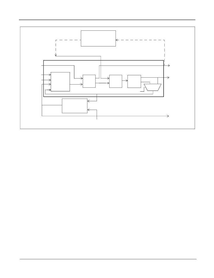
Figure 43 - Block Diagram of the Digital PLL Module
Modes of Operation (PLL_INPUT_SEL bits)
The PLL has four major modes of operation which are configured on a per-port basis via the PLL_INPUT_SEL bits
in the Clocking Configuration Registers. The four modes are, briefly, as follows:
Line-clocking mode: Synchronize to a 1.544 MHz, 2.048 MHz, or 4.096 MHz clock input to the chip on the
port’s corresponding STiCLK input line. Generate an outgoing clock with the appropriate frequency. The
outgoing service clock (1.544 MHz, 2.048 MHz, or 4.096 MHz) is phase-locked to the input clock. This mode
of operation may be used to “clean up” a jittery input clock. In line-clocking mode, the maximum locking time
is about 15 seconds.
SRTS mode: Synchronize to the incoming RTS nibbles (time stamps). Generate a 1.544 MHz, 2.048 MHz, or
4.096 MHz clock. The proper service output clock is fed into the per-port SRTS generator (outlined in
Section 4.7.2.4, “Transmit SRTS Circuit Sub-module,” on page 99) to generate a local RTS value that is
compared with subsequent received RTS values. In SRTS mode, the maximum locking time is
approximately 100 seconds.
Network mode: Similar to line-clocking mode, but the input clock is an 8 kHz clock (coming either directly
from the PHY_CLK pin or from a divided down version of a 19.44 MHz clock input at the PHY_CLK pin). The
8 kHz clock is sourced from the Clock Management module, as explained in Section 4.7.2.3, “Network Clock
Divider Circuit,” on page 97. The output clock (1.544 MHz, 2.048 MHz, or 4.096 MHz) is synchronous and
phase-locked to the 8 kHz input clock. In network mode, the maximum locking time is about 40 seconds.
Adaptive mode: Synchronize to the incoming cell stream by monitoring the fill level of a VC’s Reassembly
Circular Buffers. The PLL receives a phaseword from the UDT RX_SAR or SDT RX_SAR. A clock rate of
approximately 1.544 MHz, 2.048 MHz, or 4.096 MHz is generated, depending upon the PLL_FREQ_SEL
bits.
Note that the UDT RX_SAR and SDT RX_SAR Reassembly Control Structures must be configured appropriately if
either Adaptive or SRTS Clock Recovery methods are to be used. For more details, refer to the UDT RX_SAR and
SDT RX_SAR module descriptions in Section 4.6.1, “UDT RX_SAR and SDT RX_SAR Modules” earlier in this
document.
SRTS
Generator
*
* - outside PLL module
fnxi
Phase
Detector
Loop
Filter
DCO
Divider
RTS out
output
clock
frequency
offset
Filter implemented in
software (via CPU)
DCO_DIFF
Phaseword
Clock
Received
RTS
2:1
Mux
8 kHz_PLL
Network mode
相關PDF資料 |
PDF描述 |
|---|---|
| MT9072 | Ultraframer DS3/E3/DS2/E2/DS1/E1/DS0 |
| MT9072AB | Ultraframer DS3/E3/DS2/E2/DS1/E1/DS0 |
| MT9072AV | Ultraframer DS3/E3/DS2/E2/DS1/E1/DS0 |
| MT90820 | Large Digital Switch |
| MT90820AL | Large Digital Switch |
相關代理商/技術參數 |
參數描述 |
|---|---|
| MT90520AG2 | 制造商:Microsemi Corporation 功能描述:ATM SAR 2.048MBPS 2.5V CBR 456BGA - Trays 制造商:Zarlink Semiconductor Inc 功能描述:ATM SAR 2.048MBPS 2.5V CBR 456BGA - Trays |
| MT90528 | 制造商:ZARLINK 制造商全稱:Zarlink Semiconductor Inc 功能描述:28-Port Primary Rate Circuit Emulation AAL1 SAR |
| MT90528AG | 制造商:ZARLINK 制造商全稱:Zarlink Semiconductor Inc 功能描述:28-Port Primary Rate Circuit Emulation AAL1 SAR |
| MT90528AG2 | 制造商:ZARLINK 制造商全稱:Zarlink Semiconductor Inc 功能描述:28-Port Primary Rate Circuit Emulation AAL1 SAR |
| MT90710 | 制造商:MITEL 制造商全稱:Mitel Networks Corporation 功能描述:High-Speed Isochronous Multiplexer |
發(fā)布緊急采購,3分鐘左右您將得到回復。