- 您現(xiàn)在的位置:買(mǎi)賣(mài)IC網(wǎng) > PDF目錄384797 > OR4E14 (Lineage Power) Field-Programmable Gate Arrays(現(xiàn)場(chǎng)可編程門(mén)陣列) PDF資料下載
參數(shù)資料
| 型號(hào): | OR4E14 |
| 廠商: | Lineage Power |
| 英文描述: | Field-Programmable Gate Arrays(現(xiàn)場(chǎng)可編程門(mén)陣列) |
| 中文描述: | 現(xiàn)場(chǎng)可編程門(mén)陣列(現(xiàn)場(chǎng)可編程門(mén)陣列) |
| 文件頁(yè)數(shù): | 72/132頁(yè) |
| 文件大?。?/td> | 2667K |
| 代理商: | OR4E14 |
第1頁(yè)第2頁(yè)第3頁(yè)第4頁(yè)第5頁(yè)第6頁(yè)第7頁(yè)第8頁(yè)第9頁(yè)第10頁(yè)第11頁(yè)第12頁(yè)第13頁(yè)第14頁(yè)第15頁(yè)第16頁(yè)第17頁(yè)第18頁(yè)第19頁(yè)第20頁(yè)第21頁(yè)第22頁(yè)第23頁(yè)第24頁(yè)第25頁(yè)第26頁(yè)第27頁(yè)第28頁(yè)第29頁(yè)第30頁(yè)第31頁(yè)第32頁(yè)第33頁(yè)第34頁(yè)第35頁(yè)第36頁(yè)第37頁(yè)第38頁(yè)第39頁(yè)第40頁(yè)第41頁(yè)第42頁(yè)第43頁(yè)第44頁(yè)第45頁(yè)第46頁(yè)第47頁(yè)第48頁(yè)第49頁(yè)第50頁(yè)第51頁(yè)第52頁(yè)第53頁(yè)第54頁(yè)第55頁(yè)第56頁(yè)第57頁(yè)第58頁(yè)第59頁(yè)第60頁(yè)第61頁(yè)第62頁(yè)第63頁(yè)第64頁(yè)第65頁(yè)第66頁(yè)第67頁(yè)第68頁(yè)第69頁(yè)第70頁(yè)第71頁(yè)當(dāng)前第72頁(yè)第73頁(yè)第74頁(yè)第75頁(yè)第76頁(yè)第77頁(yè)第78頁(yè)第79頁(yè)第80頁(yè)第81頁(yè)第82頁(yè)第83頁(yè)第84頁(yè)第85頁(yè)第86頁(yè)第87頁(yè)第88頁(yè)第89頁(yè)第90頁(yè)第91頁(yè)第92頁(yè)第93頁(yè)第94頁(yè)第95頁(yè)第96頁(yè)第97頁(yè)第98頁(yè)第99頁(yè)第100頁(yè)第101頁(yè)第102頁(yè)第103頁(yè)第104頁(yè)第105頁(yè)第106頁(yè)第107頁(yè)第108頁(yè)第109頁(yè)第110頁(yè)第111頁(yè)第112頁(yè)第113頁(yè)第114頁(yè)第115頁(yè)第116頁(yè)第117頁(yè)第118頁(yè)第119頁(yè)第120頁(yè)第121頁(yè)第122頁(yè)第123頁(yè)第124頁(yè)第125頁(yè)第126頁(yè)第127頁(yè)第128頁(yè)第129頁(yè)第130頁(yè)第131頁(yè)第132頁(yè)
72
Lucent Technologies Inc.
Preliminary Data Sheet
August 2000
ORCA Series 4 FPGAs
FPGA Configuration Modes
(continued)
5-4488(F
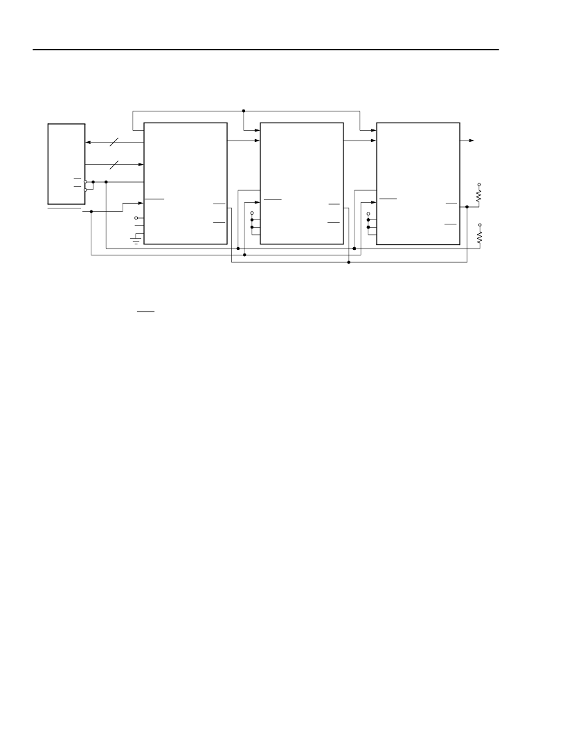
Figure 46. Daisy-Chain Configuration Schematic
V
DD
EPROM
PROGRAM
D[7:0]
OE
CE
A[17:0]
A[17:0]
D[7:0]
DONE
M2
M1
M0
DONE
HDC
LDC
RCLK
CCLK
DIN
DOUT
DOUT
DIN
CCLK
DONE
DOUT
INIT
INIT
INIT
CCLK
V
V
DD
OR
GND
PRGM
PRGM
M2
M1
M0
PRGM
M2
M1
M0
V
DD
V
DD
HDC
LDC
RCLK
HDC
LDC
RCLK
V
DD
ORCA
SERIES
FPGA
SLAVE 2
ORCA
SERIES
FPGA
MASTER
ORCA
SERIES
FPGA
SLAVE 1
As seen in Figure 46, the INIT pins for all of the FPGAs
are connected together. This is required to guarantee
that powerup and initialization will work correctly. In
general, the DONE pins for all of the FPGAs are also
connected together as shown to guarantee that all of
the FPGAs enter the start-up state simultaneously. This
may not be required, depending upon the start-up
sequence desired.
Daisy-Chaining with Boundary Scan
Multiple FPGAs can be configured through the JTAG
ports by using a daisy-chain of the FPGAs. This daisy-
chaining operation is available upon initial configuration
after powerup, after a power-on reset, after pulling the
program pin to reset the chip, or during a reconfigura-
tion if the EN_JTAG RAM has been set.
All daisy-chained FPGAs are connected in series.
Each FPGA reads and shifts the preamble and length
count in on the positive TCK and out on the negative
TCK edges.
An upstream FPGA that has received the preamble
and length count outputs a high on TDO until it has
received the appropriate number of data frames so that
downstream FPGAs do not receive frame start bit
pairs. After loading and retransmitting the preamble
and length count to a daisy chain of downstream
devices, the lead device loads its configuration data
frames.
The loading of configuration data continues after the
lead device had received its configuration read into TDI
of downstream devices on the positive edge of TCK,
and shifted out TDO on the negative edge of TCK.
Absolute Maximum Ratings
Stresses in excess of the absolute maximum ratings
can cause permanent damage to the device. These are
absolute stress ratings only. Functional operation of the
device is not implied at these or any other conditions in
excess of those given in the operations sections of this
data sheet. Exposure to absolute maximum ratings for
extended periods can adversely affect device reliability.
The ORCA Series FPGAs include circuitry designed to
protect the chips from damaging substrate injection
currents and to prevent accumulations of static charge.
Nevertheless, conventional precautions should be
observed during storage, handling, and use to avoid
exposure to excessive electrical stress.
相關(guān)PDF資料 |
PDF描述 |
|---|---|
| OR4E2 | Field-Programmable Gate Arrays(現(xiàn)場(chǎng)可編程門(mén)陣列) |
| OR4E4 | Field-Programmable Gate Arrays(現(xiàn)場(chǎng)可編程門(mén)陣列) |
| OR4E6 | Field-Programmable Gate Arrays(現(xiàn)場(chǎng)可編程門(mén)陣列) |
| ORT4622 | Field-Programmable System Chip (FPSC) Four Channel x 622 Mbits/s Backplane Transceiver(現(xiàn)場(chǎng)可編程系統(tǒng)芯片(四通道x 622 M位/秒背板收發(fā)器)) |
| ORT8850 | Field-Programmable System Chip(現(xiàn)場(chǎng)可編程系統(tǒng)芯片) |
相關(guān)代理商/技術(shù)參數(shù) |
參數(shù)描述 |
|---|---|
| OR4E2 | 制造商:AGERE 制造商全稱(chēng):AGERE 功能描述:Field-Programmable Gate Arrays |
| OR4E2-1BA256 | 制造商:未知廠家 制造商全稱(chēng):未知廠家 功能描述:FPGA |
| OR4E2-1BA352 | 制造商:未知廠家 制造商全稱(chēng):未知廠家 功能描述:FPGA |
| OR4E2-1BA416 | 制造商:未知廠家 制造商全稱(chēng):未知廠家 功能描述:FPGA |
| OR4E2-1BC432 | 制造商:未知廠家 制造商全稱(chēng):未知廠家 功能描述:FPGA |
發(fā)布緊急采購(gòu),3分鐘左右您將得到回復(fù)。