- 您現(xiàn)在的位置:買賣IC網(wǎng) > PDF目錄384797 > OR4E14 (Lineage Power) Field-Programmable Gate Arrays(現(xiàn)場可編程門陣列) PDF資料下載
參數(shù)資料
| 型號: | OR4E14 |
| 廠商: | Lineage Power |
| 英文描述: | Field-Programmable Gate Arrays(現(xiàn)場可編程門陣列) |
| 中文描述: | 現(xiàn)場可編程門陣列(現(xiàn)場可編程門陣列) |
| 文件頁數(shù): | 21/132頁 |
| 文件大小: | 2667K |
| 代理商: | OR4E14 |
第1頁第2頁第3頁第4頁第5頁第6頁第7頁第8頁第9頁第10頁第11頁第12頁第13頁第14頁第15頁第16頁第17頁第18頁第19頁第20頁當(dāng)前第21頁第22頁第23頁第24頁第25頁第26頁第27頁第28頁第29頁第30頁第31頁第32頁第33頁第34頁第35頁第36頁第37頁第38頁第39頁第40頁第41頁第42頁第43頁第44頁第45頁第46頁第47頁第48頁第49頁第50頁第51頁第52頁第53頁第54頁第55頁第56頁第57頁第58頁第59頁第60頁第61頁第62頁第63頁第64頁第65頁第66頁第67頁第68頁第69頁第70頁第71頁第72頁第73頁第74頁第75頁第76頁第77頁第78頁第79頁第80頁第81頁第82頁第83頁第84頁第85頁第86頁第87頁第88頁第89頁第90頁第91頁第92頁第93頁第94頁第95頁第96頁第97頁第98頁第99頁第100頁第101頁第102頁第103頁第104頁第105頁第106頁第107頁第108頁第109頁第110頁第111頁第112頁第113頁第114頁第115頁第116頁第117頁第118頁第119頁第120頁第121頁第122頁第123頁第124頁第125頁第126頁第127頁第128頁第129頁第130頁第131頁第132頁
Preliminary Data Sheet
August 2000
Lucent Technologies Inc.
21
ORCA Series 4 FPGAs
Programmable Logic Cells
(continued)
5-5749(F)
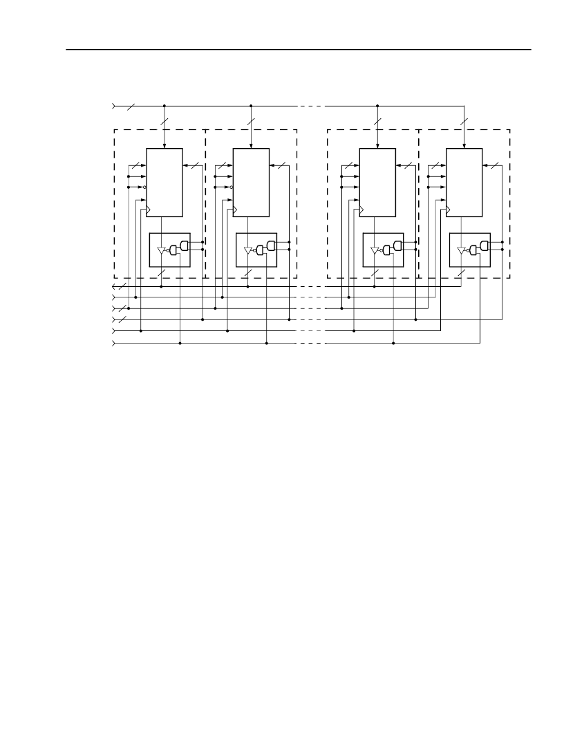
Figure 13. Memory Mode Expansion Example—128 x 8 RAM
RD[7:0]
WE
WA[6:0]
RA[6:0]
CLK
WA
RA
WPE 1
WPE 2
WE
RD[7:4]
WD[7:4]
5
5
4
PLC
8
WD[7:0]
8
7
7
WA
RA
WPE 1
WPE 2
WE
RD[3:0]
WD[3:0]
5
5
4
PLC
WA
RA
WPE 1
WPE 2
WE
RD[7:4]
WD[7:4]
5
5
4
PLC
WA
RA
WPE 1
WPE 2
WE
RD[3:0]
WD[3:0]
5
5
4
PLC
RE
RE
4
RE
4
RE
4
RE
4
Supplemental Logic and Interconnect Cell
Each PLC contains a SLIC embedded within the PLC
routing, outside of the PFU. As its name indicates, the
SLIC performs both logic and interconnect (routing)
functions. Its main features are 3-statable, bidirectional
buffers, and a PAL-like decoder capability. Figure 14
shows a diagram of a SLIC with all of its features
shown. All modes of the SLIC are not available at one
time.
The ten SLIC inputs can be sourced directly from the
PFU or from the general routing fabric. SI[0:9] inputs
can come from the horizontal or vertical routing and
I[0:9} comes from the PFU outputs O[9:0]. These
inputs can also be tied to a logical 1 or 0 constant. The
inputs are twin-quad in nature and are segregated into
two groups of four nibbles and a third group of two
inputs for control.
Each input nibble groups also have
3-state capability; however, the third pair does not.
There is one 3-state control (TRI) for each SLIC, with
the capability to invert or disable the 3-state control for
each group of four BIDIs. Separate 3-state control for
each nibble-wide group is achievable by using the
SLICs decoder (DEC) output, driven by the group of
two BIDIs, to control the 3-state of one BIDI nibble
while using the TRI signal to control the 3-state of the
other BIDI nibble. Figure 15
shows the SLIC in buffer
mode with available 3-state control from the TRI and
DEC signals. If the entire SLIC is acting in a buffer
capacity, the DEC output may be used to generate a
constant logic 1 (VHI) or logic 0 (VLO) signal for gen-
eral use.
The SLIC may also be used to generate PAL-like AND-
OR with optional INVERT (AOI) functions or a decoder
of up to 10 bits. Each group of buffers can feed into an
AND gate (4-input AND for the nibble groups and
2-input AND for the other two buffers). These AND
gates then feed into a 3-input gate that can be config-
ured as either an AND gate or an OR gate. The output
of the 3-input gate is invertible and is output at the DEC
output of the SLIC. Figure 19 shows the SLIC in full
decoder mode.
The functionality of the SLIC is parsed by the two
nibble-wide groups and the 2-bit buffer group. Each of
these groups may operate independently as BIDI buff-
ers (with or without 3-state capability for the nibble-
wide groups) or as a PAL/decoder.
相關(guān)PDF資料 |
PDF描述 |
|---|---|
| OR4E2 | Field-Programmable Gate Arrays(現(xiàn)場可編程門陣列) |
| OR4E4 | Field-Programmable Gate Arrays(現(xiàn)場可編程門陣列) |
| OR4E6 | Field-Programmable Gate Arrays(現(xiàn)場可編程門陣列) |
| ORT4622 | Field-Programmable System Chip (FPSC) Four Channel x 622 Mbits/s Backplane Transceiver(現(xiàn)場可編程系統(tǒng)芯片(四通道x 622 M位/秒背板收發(fā)器)) |
| ORT8850 | Field-Programmable System Chip(現(xiàn)場可編程系統(tǒng)芯片) |
相關(guān)代理商/技術(shù)參數(shù) |
參數(shù)描述 |
|---|---|
| OR4E2 | 制造商:AGERE 制造商全稱:AGERE 功能描述:Field-Programmable Gate Arrays |
| OR4E2-1BA256 | 制造商:未知廠家 制造商全稱:未知廠家 功能描述:FPGA |
| OR4E2-1BA352 | 制造商:未知廠家 制造商全稱:未知廠家 功能描述:FPGA |
| OR4E2-1BA416 | 制造商:未知廠家 制造商全稱:未知廠家 功能描述:FPGA |
| OR4E2-1BC432 | 制造商:未知廠家 制造商全稱:未知廠家 功能描述:FPGA |
發(fā)布緊急采購,3分鐘左右您將得到回復(fù)。