- 您現(xiàn)在的位置:買賣IC網(wǎng) > PDF目錄384797 > OR4E14 (Lineage Power) Field-Programmable Gate Arrays(現(xiàn)場可編程門陣列) PDF資料下載
參數(shù)資料
| 型號(hào): | OR4E14 |
| 廠商: | Lineage Power |
| 英文描述: | Field-Programmable Gate Arrays(現(xiàn)場可編程門陣列) |
| 中文描述: | 現(xiàn)場可編程門陣列(現(xiàn)場可編程門陣列) |
| 文件頁數(shù): | 39/132頁 |
| 文件大小: | 2667K |
| 代理商: | OR4E14 |
第1頁第2頁第3頁第4頁第5頁第6頁第7頁第8頁第9頁第10頁第11頁第12頁第13頁第14頁第15頁第16頁第17頁第18頁第19頁第20頁第21頁第22頁第23頁第24頁第25頁第26頁第27頁第28頁第29頁第30頁第31頁第32頁第33頁第34頁第35頁第36頁第37頁第38頁當(dāng)前第39頁第40頁第41頁第42頁第43頁第44頁第45頁第46頁第47頁第48頁第49頁第50頁第51頁第52頁第53頁第54頁第55頁第56頁第57頁第58頁第59頁第60頁第61頁第62頁第63頁第64頁第65頁第66頁第67頁第68頁第69頁第70頁第71頁第72頁第73頁第74頁第75頁第76頁第77頁第78頁第79頁第80頁第81頁第82頁第83頁第84頁第85頁第86頁第87頁第88頁第89頁第90頁第91頁第92頁第93頁第94頁第95頁第96頁第97頁第98頁第99頁第100頁第101頁第102頁第103頁第104頁第105頁第106頁第107頁第108頁第109頁第110頁第111頁第112頁第113頁第114頁第115頁第116頁第117頁第118頁第119頁第120頁第121頁第122頁第123頁第124頁第125頁第126頁第127頁第128頁第129頁第130頁第131頁第132頁
Lucent Technologies Inc.
39
Preliminary Data Sheet
August 2000
ORCA Series 4 FPGAs
Special Function Blocks
(continued)
Temperature Sensing
The built-in temperature-sensing diodes allow junction
temperature to be measured during device operation. A
physical pin (PTEMP) is dedicated for monitoring
device junction temperature. PTEMP works by forcing a
10 mA current in the forward direction, and then mea-
suring the resulting voltage. The voltage decreases
with increasing temperature at approximately
–1.69 mV/°C. A typical device with a 85 °C device tem-
perature will measure approximately 630 mV.
Table 21. Dedicated Temperature Sensing
Boundary-Scan
The IEEE standards 1149.1 and 1149.2 (IEEE Stan-
dard test access port and boundary-scan architecture)
are implemented in the ORCA series of FPGAs. It
allows users to efficiently test the interconnection
between integrated circuits on a PCB as well as test the
integrated circuit itself. The IEEE1149 standard is a
well-defined protocol that ensures interoperability
among boundary-scan (BSCAN) equipped devices
from different vendors.
Series 4 FPGAs are also compliant to IEEE standard
1532/D1. This standard for boundary-scan based in-
system configuration of programmable devices pro-
vides a standardized programming access and method-
ology for FPGAs. A device, or set of devices,
implementing this standard may be programmed, read
back, erased verified, singly or concurrently, with a
standard set of resources.
The IEEE 1149 standards define a test access port
(TAP) that consists of a four-pin interface with an
optional reset pin for boundary-scan testing of inte-
grated circuits in a system. The ORCA Series FPGA
provides four interface pins: test data in (TDI), test
mode select (TMS), test clock (TCK), and test data out
(TDO). The
PRGM
pin used to reconfigure the device
also resets the boundary-scan logic.
The user test host serially loads test commands and
test data into the FPGA through these pins to drive out-
puts and examine inputs. In the configuration shown in
Figure 26, where boundary-scan is used to test ICs,
test data is transmitted serially into TDI of the first
BSCAN device (U1), through TDO/TDI connections
between BSCAN devices (U2 and U3), and out TDO of
the last BSCAN device (U4). In this configuration, the
TMS and TCK signals are routed to all boundary-scan
ICs in parallel so that all boundary-scan components
operate in the same state. In other configurations, mul-
tiple scan paths are used instead of a single ring. When
multiple scan paths are used, each ring is indepen-
dently controlled by its own TMS and TCK signals.
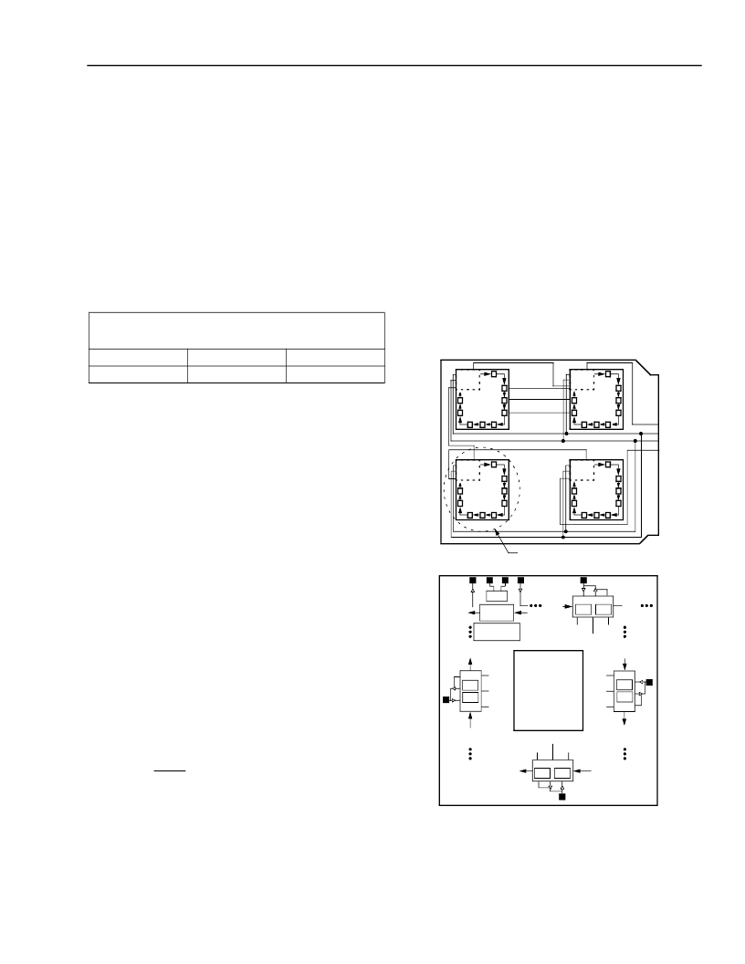
Figure 26 provides a system interface for components
used in the boundary-scan testing of PCBs. The three
major components shown are the test host, boundary-
scan support circuit, and the devices under test
(DUTs). The DUTs shown here are ORCA Series
FPGAs with dedicated boundary-scan circuitry. The
test host is normally one of the following: automatic test
equipment (ATE), a workstation, a PC, or a micropro-
cessor.
5-5972(F)
Key: BSC = boundary-scan cell, BDC = bidirectional data cell, and
DCC = data control cell.
Figure 25. Printed-Circuit Board with Boundary-
Scan Circuitry
Dedicated Temperature Sensing Diode Pin Per
Package
BA352
BC432
AB3
AH31
BM680
AK4
INSTRUCTION
REGISTER
TDO
BYPASS
REGISTER
TCK TMS TDI
SCAN
OUT
SCAN
IN
SCAN
OUT
SCAN
IN
SCAN
IN
SCAN
OUT
BSC
BDC
DCC
SCAN
OUT
SCAN
IN
TAPC
p_in
p_in
p_out
p_in
p_ts
p_out
p_ts
p_in
p_out
p_ts
p_out
p_ts
PL[ij]
PT[ij]
PR[ij]
PB[ij]
BDC
DCC
PLC
ARRAY
BDC
DCC
BDC
DCC
BSC
BSC
BSC
SEE ENLARGED VIEW BELOW.
TMS TDI
TCK
TDO
TMS TDI
TCK
TDO
TMS TDI
TCK
TDO
TMS TDI
TCK
TDO
U1
U2
U3
U4
TDI
TCK
TDO
TMS
net a
net b
net c
S
相關(guān)PDF資料 |
PDF描述 |
|---|---|
| OR4E2 | Field-Programmable Gate Arrays(現(xiàn)場可編程門陣列) |
| OR4E4 | Field-Programmable Gate Arrays(現(xiàn)場可編程門陣列) |
| OR4E6 | Field-Programmable Gate Arrays(現(xiàn)場可編程門陣列) |
| ORT4622 | Field-Programmable System Chip (FPSC) Four Channel x 622 Mbits/s Backplane Transceiver(現(xiàn)場可編程系統(tǒng)芯片(四通道x 622 M位/秒背板收發(fā)器)) |
| ORT8850 | Field-Programmable System Chip(現(xiàn)場可編程系統(tǒng)芯片) |
相關(guān)代理商/技術(shù)參數(shù) |
參數(shù)描述 |
|---|---|
| OR4E2 | 制造商:AGERE 制造商全稱:AGERE 功能描述:Field-Programmable Gate Arrays |
| OR4E2-1BA256 | 制造商:未知廠家 制造商全稱:未知廠家 功能描述:FPGA |
| OR4E2-1BA352 | 制造商:未知廠家 制造商全稱:未知廠家 功能描述:FPGA |
| OR4E2-1BA416 | 制造商:未知廠家 制造商全稱:未知廠家 功能描述:FPGA |
| OR4E2-1BC432 | 制造商:未知廠家 制造商全稱:未知廠家 功能描述:FPGA |
發(fā)布緊急采購,3分鐘左右您將得到回復(fù)。