- 您現(xiàn)在的位置:買賣IC網(wǎng) > PDF目錄299156 > GE28F640W30TD70 (INTEL CORP) 4M X 16 FLASH 1.8V PROM, 70 ns, PBGA56 PDF資料下載
參數(shù)資料
| 型號: | GE28F640W30TD70 |
| 廠商: | INTEL CORP |
| 元件分類: | PROM |
| 英文描述: | 4M X 16 FLASH 1.8V PROM, 70 ns, PBGA56 |
| 封裝: | 0.75 MM PITCH, VFBGA-56 |
| 文件頁數(shù): | 3/104頁 |
| 文件大小: | 1443K |
| 代理商: | GE28F640W30TD70 |
第1頁第2頁當(dāng)前第3頁第4頁第5頁第6頁第7頁第8頁第9頁第10頁第11頁第12頁第13頁第14頁第15頁第16頁第17頁第18頁第19頁第20頁第21頁第22頁第23頁第24頁第25頁第26頁第27頁第28頁第29頁第30頁第31頁第32頁第33頁第34頁第35頁第36頁第37頁第38頁第39頁第40頁第41頁第42頁第43頁第44頁第45頁第46頁第47頁第48頁第49頁第50頁第51頁第52頁第53頁第54頁第55頁第56頁第57頁第58頁第59頁第60頁第61頁第62頁第63頁第64頁第65頁第66頁第67頁第68頁第69頁第70頁第71頁第72頁第73頁第74頁第75頁第76頁第77頁第78頁第79頁第80頁第81頁第82頁第83頁第84頁第85頁第86頁第87頁第88頁第89頁第90頁第91頁第92頁第93頁第94頁第95頁第96頁第97頁第98頁第99頁第100頁第101頁第102頁第103頁第104頁
28F640W30, 28F320W30, 28F128W30
June 2005
Intel Wireless Flash Memory (W30)
Datasheet
100
Order Number: 290702, Revision: 011
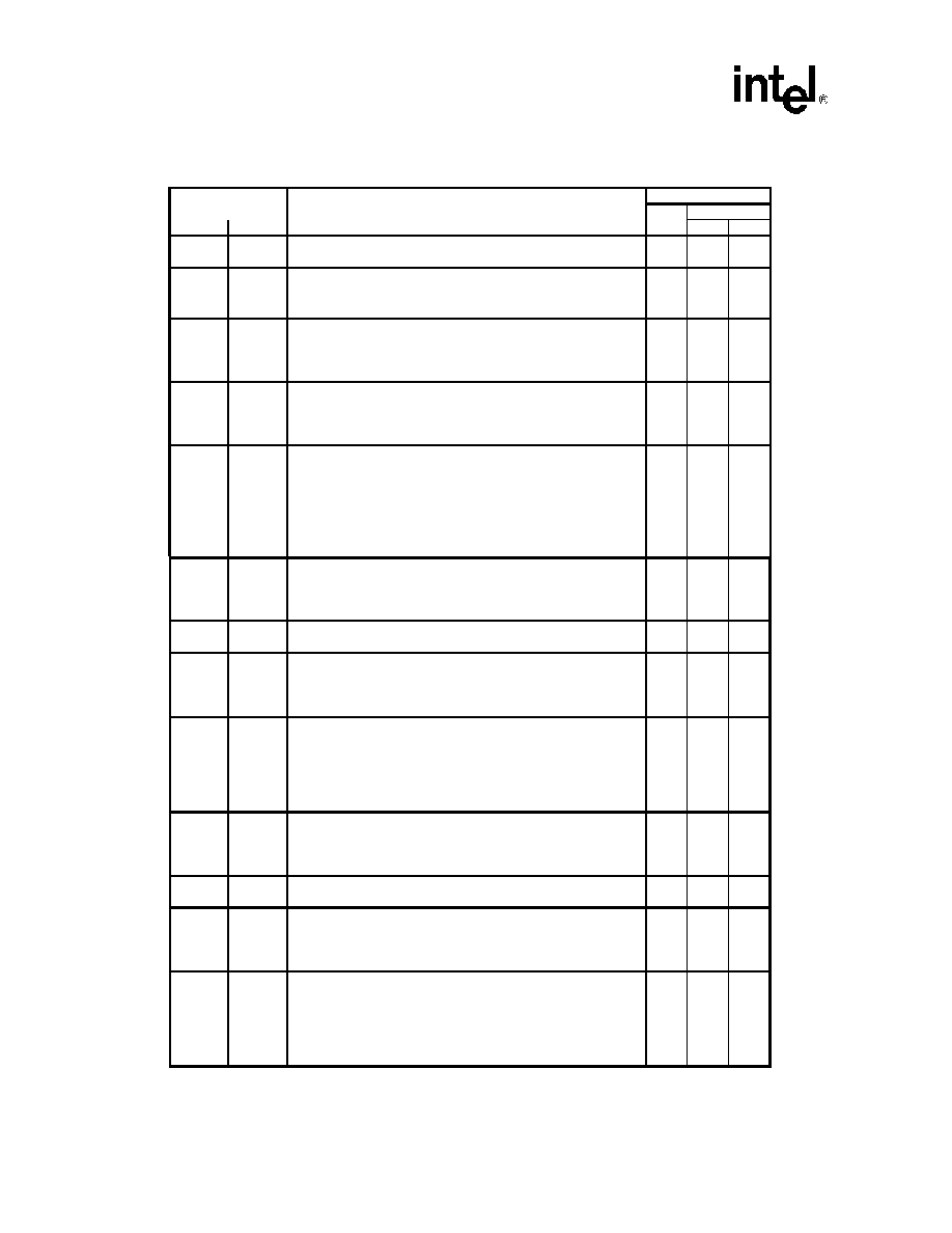
Table 43.
Partition Region 1 Information
Offset
(1)
See table below
P = 39h
Description
Address
Bottom
Top
(Optional flash features and commands)
Len
Bot
Top
(P+1A)h
(P+1A)h Number of identical partitions within the partition region
2
53:
(P+1B)h
54:
(P+1C)h
1
55:
(P+1D)h
1
56:
(P+1E)h
1
57:
(P+1F)h
1
58:
(P+20)h
(P+20)h Partition Region 1 Erase Block Type 1 Information
4
59:
(P+21)h
bits 0–15 = y, y+1 = number of identical-size erase blocks
5A:
(P+22)h
bits 16–31 = z, region erase block(s) size are z x 256 bytes
5B:
(P+23)h
5C:
(P+24)h
(P+24)h Partition 1 (Erase Block Type 1)
25D:
5D:
(P+25)h
Minimum block erase cycles x 1000
5E:
(P+26)h
1
5F:
(P+27)h
1
60:
(P+28)h
Partition Region 1 Erase Block Type 2 Information
4
61:
(P+29)h
bits 0–15 = y, y+1 = number of identical-size erase blocks
62:
(P+2A)h
bits 16–31 = z, region erase block(s) size are z x 256 bytes
63:
(P+2B)h
(bottom parameter device only)
64:
(P+2C)h
Partition 1 (Erase block Type 2)
2
65:
(P+2D)h
Minimum block erase cycles x 1000
66:
(P+2E)h
167:
(P+2F)h
168:
partitions while a partition in this region is in Program mode
bits 0–3 = number of simultaneous Program operations
bits 4–7 = number of simultaneous Erase operations
Simultaneous program or erase operations allowed in other
partitions while a partition in this region is in Erase mode
bits 0–3 = number of simultaneous Program operations
bits 4–7 = number of simultaneous Erase operations
Number of program or erase operations allowed in a partition
bits 0–3 = number of simultaneous Program operations
bits 4–7 = number of simultaneous Erase operations
Partition 1 (erase block Type 1) bits per cell; internal ECC
bits 0–3 = bits per cell in erase region
bit 4 = reserved for “internal ECC used” (1=yes, 0=no)
bits 5–7 = reserve for future use
Partition 1 (erase block Type 1) page mode and synchronous
mode capabilities defined in Table 10.
bit 0 = page-mode host reads permitted (1=yes, 0=no)
bit 1 = synchronous host reads permitted (1=yes, 0=no)
bit 2 = synchronous host writes permitted (1=yes, 0=no)
bits 3–7 = reserved for future use
Partition 1 (Erase block Type 2) bits per cell
bits 0–3 = bits per cell in erase region
bit 4 = reserved for “internal ECC used” (1=yes, 0=no)
bits 5–7 = reserve for future use
Partition 1 (Erase block Type 2) pagemode and synchronous
mode capabilities defined in Table 10
bit 0 = page-mode host reads permitted (1=yes, 0=no)
bit 1 = synchronous host reads permitted (1=yes, 0=no)
bit 2 = synchronous host writes permitted (1=yes, 0=no)
bits 3–7 = reserved for future use
Types of erase block regions in this Partition Region.
x = 0 = no erase blocking; the Partition Region erases in bulk
x = number of erase block regions w/ contiguous same-size
erase blocks. Symmetrically blocked partitions have one
blocking region. Partition size = (Type 1 blocks)x(Type 1
block sizes) + (Type 2 blocks)x(Type 2 block sizes) +…+
(Type n blocks)x(Type n block sizes)
相關(guān)PDF資料 |
PDF描述 |
|---|---|
| GEN12.5-120 | Programmable DC Power Supplies 750W/1500W |
| GEN12.5-60 | Programmable DC Power Supplies 750W/1500W |
| GFL750 | COPPER ALLOY, WIRE TERMINAL |
| GFL500 | COPPER ALLOY, WIRE TERMINAL |
| GFL350 | COPPER ALLOY, WIRE TERMINAL |
相關(guān)代理商/技術(shù)參數(shù) |
參數(shù)描述 |
|---|---|
| GE28F800B3BA90 | 制造商:Intel 功能描述:NOR Flash, 512K x 16, 45 Pin, Plastic, BGA |
| GE28F800B3TA90 | 制造商:INTEL 制造商全稱:Intel Corporation 功能描述:3 Volt Advanced Boot Block Flash Memory |
| GE28F800C3BA70 | 制造商:INTEL 制造商全稱:Intel Corporation 功能描述:Advanced+ Boot Block Flash Memory (C3) |
| GE28F800C3BA90 | 制造商:INTEL 制造商全稱:Intel Corporation 功能描述:Advanced+ Boot Block Flash Memory (C3) |
| GE28F800C3BC70 | 制造商:INTEL 制造商全稱:Intel Corporation 功能描述:Advanced+ Boot Block Flash Memory (C3) |
發(fā)布緊急采購,3分鐘左右您將得到回復(fù)。