- 您現(xiàn)在的位置:買賣IC網(wǎng) > PDF目錄299156 > GE28F640W30TD70 (INTEL CORP) 4M X 16 FLASH 1.8V PROM, 70 ns, PBGA56 PDF資料下載
參數(shù)資料
| 型號(hào): | GE28F640W30TD70 |
| 廠商: | INTEL CORP |
| 元件分類: | PROM |
| 英文描述: | 4M X 16 FLASH 1.8V PROM, 70 ns, PBGA56 |
| 封裝: | 0.75 MM PITCH, VFBGA-56 |
| 文件頁(yè)數(shù): | 104/104頁(yè) |
| 文件大小: | 1443K |
| 代理商: | GE28F640W30TD70 |
第1頁(yè)第2頁(yè)第3頁(yè)第4頁(yè)第5頁(yè)第6頁(yè)第7頁(yè)第8頁(yè)第9頁(yè)第10頁(yè)第11頁(yè)第12頁(yè)第13頁(yè)第14頁(yè)第15頁(yè)第16頁(yè)第17頁(yè)第18頁(yè)第19頁(yè)第20頁(yè)第21頁(yè)第22頁(yè)第23頁(yè)第24頁(yè)第25頁(yè)第26頁(yè)第27頁(yè)第28頁(yè)第29頁(yè)第30頁(yè)第31頁(yè)第32頁(yè)第33頁(yè)第34頁(yè)第35頁(yè)第36頁(yè)第37頁(yè)第38頁(yè)第39頁(yè)第40頁(yè)第41頁(yè)第42頁(yè)第43頁(yè)第44頁(yè)第45頁(yè)第46頁(yè)第47頁(yè)第48頁(yè)第49頁(yè)第50頁(yè)第51頁(yè)第52頁(yè)第53頁(yè)第54頁(yè)第55頁(yè)第56頁(yè)第57頁(yè)第58頁(yè)第59頁(yè)第60頁(yè)第61頁(yè)第62頁(yè)第63頁(yè)第64頁(yè)第65頁(yè)第66頁(yè)第67頁(yè)第68頁(yè)第69頁(yè)第70頁(yè)第71頁(yè)第72頁(yè)第73頁(yè)第74頁(yè)第75頁(yè)第76頁(yè)第77頁(yè)第78頁(yè)第79頁(yè)第80頁(yè)第81頁(yè)第82頁(yè)第83頁(yè)第84頁(yè)第85頁(yè)第86頁(yè)第87頁(yè)第88頁(yè)第89頁(yè)第90頁(yè)第91頁(yè)第92頁(yè)第93頁(yè)第94頁(yè)第95頁(yè)第96頁(yè)第97頁(yè)第98頁(yè)第99頁(yè)第100頁(yè)第101頁(yè)第102頁(yè)第103頁(yè)當(dāng)前第104頁(yè)
28F640W30, 28F320W30, 28F128W30
Datasheet
Intel Wireless Flash Memory (W30)
June 2005
Order Number: 290702, Revision: 011
99
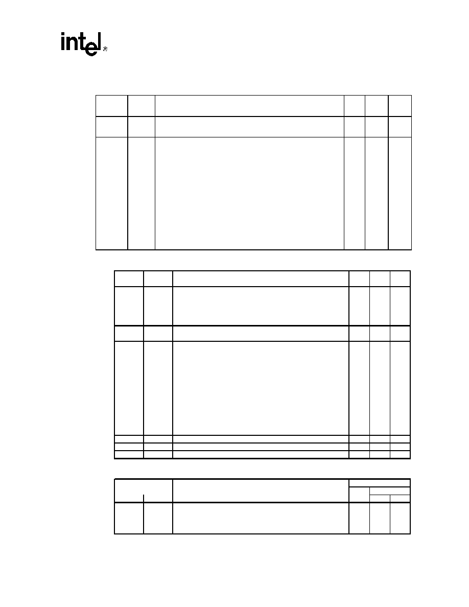
Table 41.
Burst Read Information for Non-Multiplexed Flash Device
Table 42.
Partition and Erase-Block Region Information
Table 40.
Protection Register Information
Offset(1)
P = 39h
Length
Description (Optional flash device features and commands)
Add.
Hex
Code
Value
(P+E)h
1
Number of Protection register fields in JEDEC ID space.
00h indicates that 256 protection fields are available
47:
--01
1
(P+F)h
(P+10)h
(P+11)h
(P+12)h
4
Protection Field 1: Protection Description
This field describes user-available One Time Programmable (OTP)
Protection register bytes.
Some bytes are pre-programmed with flash device-unique
serial numbers.
Other bytes are user programmable.
Bits 0-15 point to the Protection register Lock byte, the first byte in
the section. The following bytes are factory pre-programmed and
user-programmable.
bits 0--7 = Lock/bytes Jedec-plane physical low address
bits 8--15 = Lock/bytes Jedec-plane physical high address
bits 16--23 = n such that 2n = factory pre-programmed bytes
bits 24--31 =n such that 2n = user programmable bytes
48:
49:
4A:
4B:
--80
--00
--03
80h
00h
8 byte
Offset
(1)
Length
Description
Hex
P = 39h
(Optional flash features and commands)
Add.
Code Value
(P+13)h
1
4C:
--03
8 byte
(P+14)h
1
4D:
--04
4
(P+15)h
1
4E:
--01
4
(P+16)h
1
Synchronous mode read capability configuration 2
4F:
--02
8
(P+17)h
1
Synchronous mode read capability configuration 3
50:
--03
16
(P+18)h
1
Synchronous mode read capability configuration 4
51:
--07
Cont
Page Mode Read capability
bits 0–7 = “n” such that 2
n HEX value represents the number of
read-page bytes. See offset 28h for device word width to
determine page-mode data output width. 00h indicates no
read page buffer.
Number of synchronous mode read configuration fields that
follow. 00h indicates no burst capability.
Synchronous mode read capability configuration 1
Bits 3–7 = Reserved
bits 0–2 “n” such that 2
n+1 HEX value represents the
maximum number of continuous synchronous reads when
the device is configured for its maximum word width. A value
of 07h indicates that the device is capable of continuous
linear bursts that will output data until the internal burst
counter reaches the end of the device’s burstable address
space. This field’s 3-bit value can be written directly to the
Read Configuration Register bits 0–2 if the device is
configured for its maximum word width. See offset 28h for
word width to determine the burst data output width.
Offset
(1)
See table below
P = 39h
Description
Address
Bottom
Top
(Optional flash features and commands)
Len
Bot
Top
(P+19)h
1
52:
Number of device hardware-partition regions within the device.
x = 0: a single hardware partition device (no fields follow).
x specifies the number of device partition regions containing
one or more contiguous erase block regions.
相關(guān)PDF資料 |
PDF描述 |
|---|---|
| GEN12.5-120 | Programmable DC Power Supplies 750W/1500W |
| GEN12.5-60 | Programmable DC Power Supplies 750W/1500W |
| GFL750 | COPPER ALLOY, WIRE TERMINAL |
| GFL500 | COPPER ALLOY, WIRE TERMINAL |
| GFL350 | COPPER ALLOY, WIRE TERMINAL |
相關(guān)代理商/技術(shù)參數(shù) |
參數(shù)描述 |
|---|---|
| GE28F800B3BA90 | 制造商:Intel 功能描述:NOR Flash, 512K x 16, 45 Pin, Plastic, BGA |
| GE28F800B3TA90 | 制造商:INTEL 制造商全稱:Intel Corporation 功能描述:3 Volt Advanced Boot Block Flash Memory |
| GE28F800C3BA70 | 制造商:INTEL 制造商全稱:Intel Corporation 功能描述:Advanced+ Boot Block Flash Memory (C3) |
| GE28F800C3BA90 | 制造商:INTEL 制造商全稱:Intel Corporation 功能描述:Advanced+ Boot Block Flash Memory (C3) |
| GE28F800C3BC70 | 制造商:INTEL 制造商全稱:Intel Corporation 功能描述:Advanced+ Boot Block Flash Memory (C3) |
發(fā)布緊急采購(gòu),3分鐘左右您將得到回復(fù)。