- 您現(xiàn)在的位置:買賣IC網(wǎng) > PDF目錄98068 > S1C6N3B0D0A0100 MICROCONTROLLER, UUC54 PDF資料下載
參數(shù)資料
| 型號(hào): | S1C6N3B0D0A0100 |
| 元件分類: | 微控制器/微處理器 |
| 英文描述: | MICROCONTROLLER, UUC54 |
| 封裝: | DIE-54 |
| 文件頁(yè)數(shù): | 6/79頁(yè) |
| 文件大小: | 606K |
| 代理商: | S1C6N3B0D0A0100 |
第1頁(yè)第2頁(yè)第3頁(yè)第4頁(yè)第5頁(yè)當(dāng)前第6頁(yè)第7頁(yè)第8頁(yè)第9頁(yè)第10頁(yè)第11頁(yè)第12頁(yè)第13頁(yè)第14頁(yè)第15頁(yè)第16頁(yè)第17頁(yè)第18頁(yè)第19頁(yè)第20頁(yè)第21頁(yè)第22頁(yè)第23頁(yè)第24頁(yè)第25頁(yè)第26頁(yè)第27頁(yè)第28頁(yè)第29頁(yè)第30頁(yè)第31頁(yè)第32頁(yè)第33頁(yè)第34頁(yè)第35頁(yè)第36頁(yè)第37頁(yè)第38頁(yè)第39頁(yè)第40頁(yè)第41頁(yè)第42頁(yè)第43頁(yè)第44頁(yè)第45頁(yè)第46頁(yè)第47頁(yè)第48頁(yè)第49頁(yè)第50頁(yè)第51頁(yè)第52頁(yè)第53頁(yè)第54頁(yè)第55頁(yè)第56頁(yè)第57頁(yè)第58頁(yè)第59頁(yè)第60頁(yè)第61頁(yè)第62頁(yè)第63頁(yè)第64頁(yè)第65頁(yè)第66頁(yè)第67頁(yè)第68頁(yè)第69頁(yè)第70頁(yè)第71頁(yè)第72頁(yè)第73頁(yè)第74頁(yè)第75頁(yè)第76頁(yè)第77頁(yè)第78頁(yè)第79頁(yè)
6
EPSON
S1C6N3B0 TECHNICAL MANUAL
CHAPTER 2: POWER SUPPLY AND INITIAL RESET
2.1.1 Voltage <VD1> for oscillation circuit and internal circuits
VD1 is a voltage for the oscillation circuit and the internal logic circuits.
VD1 is driven with the supply voltage VDD in the normal operating mode.
The S1C6N3B0 can be set in the heavy load protection mode to protect the IC operation from voltage
variation when heavy loads such as a buzzer is driven and to operate in a condition of VDD
≤ 1.1 V (see
Section 4.10 for detail). In the heavy protection mode, the S1C6N3B0 drives VD1 with the boosted voltage
VC2 (explained in the next section) for stabilizing operation in low supply voltage.
The S1C6A3B0 always drives VD1 with the supply voltage VDD.
2.1.2 Voltage <VC1–VC3> for LCD driving
VC1–VC3 are the LCD drive voltages. They can be generated by the internal LCD system power supply
circuit or can be supplied from outside by selecting mask option.
The LCD system power supply circuit consists of two voltage circuits: a voltage regulator that generates
the VC1 voltage and a voltage booster circuit that generates the VC2 and VC3 voltages by doubling and
tripling the VC1 (when the internal voltage regulator is selected as the LCD power source by mask
option).
The LCD system power supply circuit stops operating in the SLEEP mode (available for the CR oscilla-
tion model of the S1C6N3B0 and S1C6A3B0). The voltages VC1 to VC3 go to VSS level when it stops. (The
SLEEP function cannot be used when an external LCD power supply is selected.)
In the heavy load protection mode in the S1C6N3B0, the VC2 is also used for driving the oscillation
system voltage regulator.
2.2 Initial Reset
To initialize the S1C6N3B0 Series circuits, an initial reset must be executed. There are three ways of doing
this.
(1) External initial reset by simultaneous low input to terminals K00–K03 (depending on mask option)
(2) External initial reset via the RESET terminal
(3) Initial reset by the oscillation detection circuit
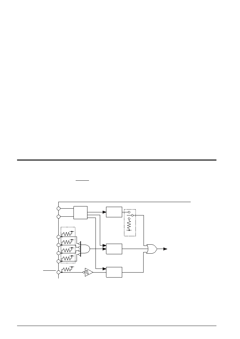
Figure 2.2.1 shows the configuration of the initial reset circuit.
RESET
K00
K01
K02
K03
OSC2
OSC1
oscilation
circuit
Noise
reject
circuit
Latch
Internal
initial reset
"L" when SLEEP function is selected
VDD
Oscillation
detection
circuit
VDD
VSS
Mask option
Fig. 2.2.1 Configuration of initial reset circuit
2.2.1 Simultaneous low input to input ports (K00–K03)
An initial reset can be performed by inputting low signals simultaneously to the input ports (K00–K03)
selected with the mask option. The specified input port terminals must be kept low for at least a time
shown in Table 2.2.1.1, because the signals pass through the noise rejection circuit. Table 2.2.1.2 shows the
combinations of the input ports (K00–K03) that can be selected with the mask option.
相關(guān)PDF資料 |
PDF描述 |
|---|---|
| S1C6P366D0A0100 | 4-BIT, FLASH, 4.1 MHz, MICROCONTROLLER, UUC102 |
| S1C6P466D0A0A00 | MICROCONTROLLER, UUC140 |
| S1C6S2L7D | 4-BIT, MROM, 0.032 MHz, MICROCONTROLLER, UUC58 |
| S1C6S2A7F | 4-BIT, MROM, 0.08 MHz, MICROCONTROLLER, PQFP60 |
| S1C6S2B7F | 4-BIT, MROM, 0.08 MHz, MICROCONTROLLER, PQFP60 |
相關(guān)代理商/技術(shù)參數(shù) |
參數(shù)描述 |
|---|---|
| S1C-6-S | 制造商:GRIPCO 功能描述: |
| S1C7309X | 制造商:SAMSUNG 制造商全稱:Samsung semiconductor 功能描述:B/W CCD PROCESSOR |
| S1C7309X01 | 制造商:SAMSUNG 制造商全稱:Samsung semiconductor 功能描述:B/W CCD PROCESSOR |
| S1C88349 | 制造商:EPSON 制造商全稱:EPSON 功能描述:8-bit Single Chip Microcomputer |
| S1C88649 | 制造商:EPSON 制造商全稱:EPSON 功能描述:8-bit Single Chip Microcomputer |
發(fā)布緊急采購(gòu),3分鐘左右您將得到回復(fù)。