- 您現(xiàn)在的位置:買賣IC網(wǎng) > PDF目錄98068 > S1C6N3B0D0A0100 MICROCONTROLLER, UUC54 PDF資料下載
參數(shù)資料
| 型號(hào): | S1C6N3B0D0A0100 |
| 元件分類: | 微控制器/微處理器 |
| 英文描述: | MICROCONTROLLER, UUC54 |
| 封裝: | DIE-54 |
| 文件頁數(shù): | 38/79頁 |
| 文件大?。?/td> | 606K |
| 代理商: | S1C6N3B0D0A0100 |
第1頁第2頁第3頁第4頁第5頁第6頁第7頁第8頁第9頁第10頁第11頁第12頁第13頁第14頁第15頁第16頁第17頁第18頁第19頁第20頁第21頁第22頁第23頁第24頁第25頁第26頁第27頁第28頁第29頁第30頁第31頁第32頁第33頁第34頁第35頁第36頁第37頁當(dāng)前第38頁第39頁第40頁第41頁第42頁第43頁第44頁第45頁第46頁第47頁第48頁第49頁第50頁第51頁第52頁第53頁第54頁第55頁第56頁第57頁第58頁第59頁第60頁第61頁第62頁第63頁第64頁第65頁第66頁第67頁第68頁第69頁第70頁第71頁第72頁第73頁第74頁第75頁第76頁第77頁第78頁第79頁
S1C6N3B0 TECHNICAL MANUAL
EPSON
35
CHAPTER 4: PERIPHERAL CIARCUITS AND OPERATION (LCD Driver)
4.6.5 Control of LCD driver
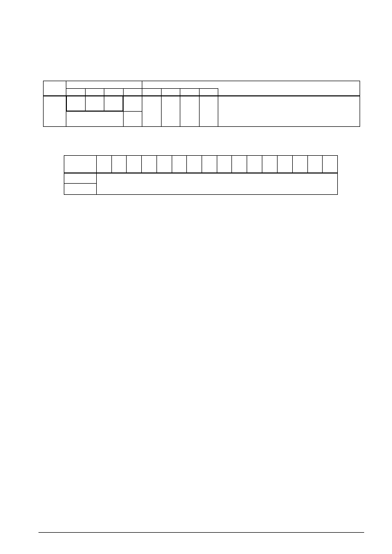
Table 4.6.5.1 shows the control bits of the LCD driver and their addresses. Figure 4.6.5.1 shows the
display memory map.
Table 4.6.5.1 I/O memory (LCD driver)
Address
Comment
D3
D2
Register
D1
D0
Name
Init 1
10
0FBH
CSDC ALLOFF ALLON
0
R/W
R
CSDC
ALLOFF
ALLON
0 3
0
1
0
– 2
Static
All Off
All On
–
Dynamic
Normal
–
LCD drive mode switch
LCD all-off control
LCD all-on control
Unused
1
2
Initial value at initial reset
Not set in the circuit
3
4
Always "0" being read
Reset (0) immediately after being read
Address
01
234
567
89
A
B
C
D
E
F
090
0A0
Display memory (W only)
32 words
× 4 bits
Fig. 4.6.5.1 Display memory map
CSDC: LCD drive switch (0FBH D3)
Selects the LCD drive method.
When "1" is written: Static drive
When "0" is written: Dynamic drive
Reading: Valid
At initial reset, this register is set to "0".
ALLOFF: LCD all OFF control register (0FBH D2)
Fade outs the all LCD segments.
When "1" is written: All LCD segments fade out
When "0" is written: Normal display
Reading: Valid
By writing "1" to the ALLOFF register, all the LCD segments goes off, and when "0" is written, it returns
to normal display. This function does not affect the contents of the display memory.
At initial reset, this register is set to "1".
ALLON: LCD all ON control register (0FBH D1)
Displays the all LCD segments on.
When "1" is written: All LCD segments displayed
When "0" is written: Normal display
Reading: Valid
By writing "1" to the ALLON register, all the LCD segments goes on, and when "0" is written, it returns to
normal display. This function does not affect the contents of the display memory.
At initial reset, this register is set to "0".
相關(guān)PDF資料 |
PDF描述 |
|---|---|
| S1C6P366D0A0100 | 4-BIT, FLASH, 4.1 MHz, MICROCONTROLLER, UUC102 |
| S1C6P466D0A0A00 | MICROCONTROLLER, UUC140 |
| S1C6S2L7D | 4-BIT, MROM, 0.032 MHz, MICROCONTROLLER, UUC58 |
| S1C6S2A7F | 4-BIT, MROM, 0.08 MHz, MICROCONTROLLER, PQFP60 |
| S1C6S2B7F | 4-BIT, MROM, 0.08 MHz, MICROCONTROLLER, PQFP60 |
相關(guān)代理商/技術(shù)參數(shù) |
參數(shù)描述 |
|---|---|
| S1C-6-S | 制造商:GRIPCO 功能描述: |
| S1C7309X | 制造商:SAMSUNG 制造商全稱:Samsung semiconductor 功能描述:B/W CCD PROCESSOR |
| S1C7309X01 | 制造商:SAMSUNG 制造商全稱:Samsung semiconductor 功能描述:B/W CCD PROCESSOR |
| S1C88349 | 制造商:EPSON 制造商全稱:EPSON 功能描述:8-bit Single Chip Microcomputer |
| S1C88649 | 制造商:EPSON 制造商全稱:EPSON 功能描述:8-bit Single Chip Microcomputer |
發(fā)布緊急采購(gòu),3分鐘左右您將得到回復(fù)。