- 您現(xiàn)在的位置:買賣IC網(wǎng) > PDF目錄164343 > 8D0-25W20AA022 (SOURIAU INC) 30 CONTACT(S), ALUMINUM ALLOY, MALE, MIL SERIES CONNECTOR, CRIMP, RECEPTACLE PDF資料下載
參數(shù)資料
| 型號: | 8D0-25W20AA022 |
| 廠商: | SOURIAU INC |
| 元件分類: | MIL系列連接器 |
| 英文描述: | 30 CONTACT(S), ALUMINUM ALLOY, MALE, MIL SERIES CONNECTOR, CRIMP, RECEPTACLE |
| 文件頁數(shù): | 2/12頁 |
| 文件大小: | 692K |
| 代理商: | 8D0-25W20AA022 |
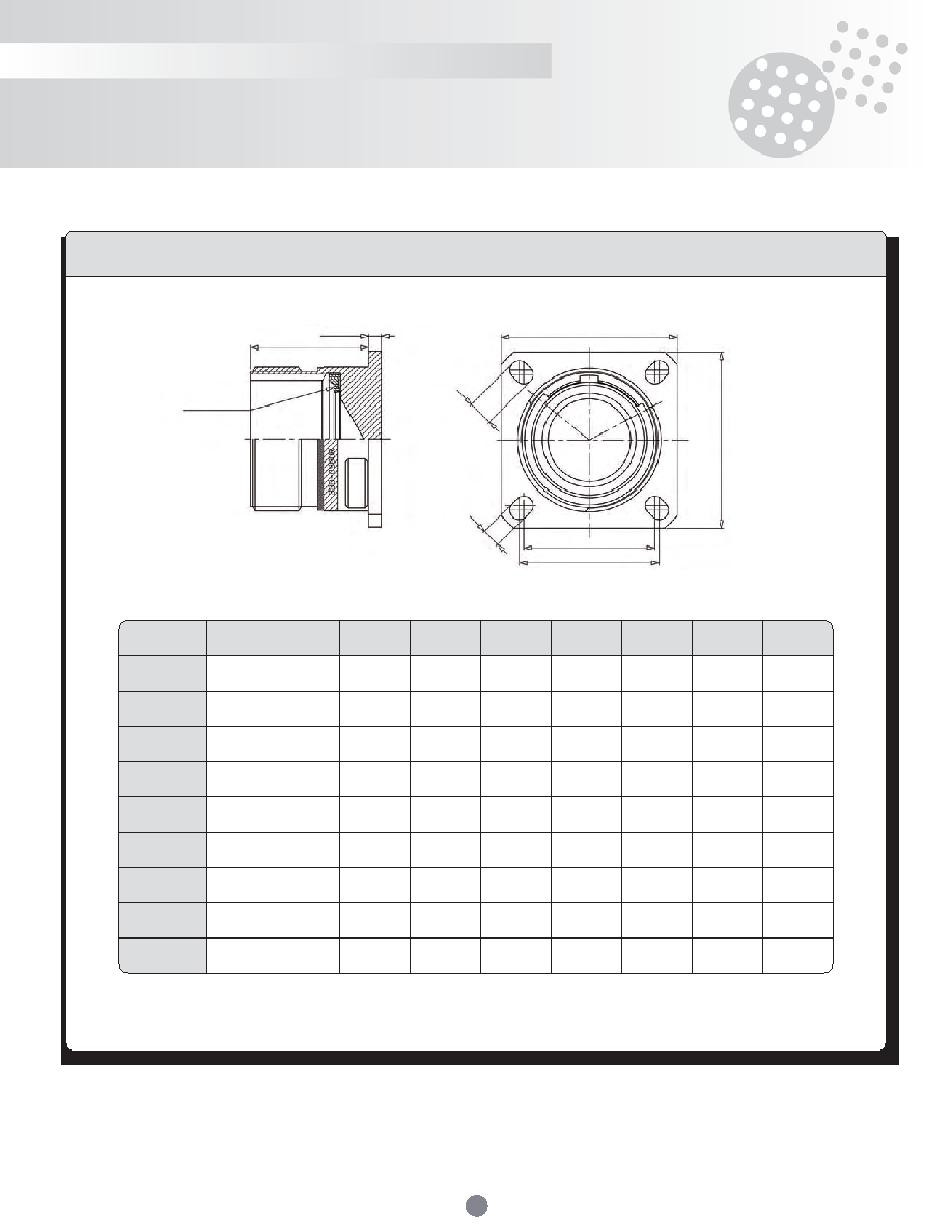
31
8D Series
D38999 Aluminum Series
Dimensions
Coupling joint
A
B
C
E
D
F
G
Shell size
Souriau
Part number *
A Max
B Max
C±0.30
D
E
F±0.20
G±0.20
09
8D0-09GUR
8D0-09FUR
20.90
2.50
23.80
18.26
15.09
4.49
3.25
11
8D0-11GUR
8D0-11FUR
20.90
2.50
26.20
20.62
18.26
4.93
3.25
13
8D0-13GUR
8D0-13FUR
20.90
2.50
28.60
23.01
20.62
4.93
3.25
15
8D0-15GUR
8D0-15FUR
20.90
2.50
31.00
24.61
23.01
4.93
3.25
17
8D0-17GUR
8D0-17FUR
20.90
2.50
33.30
26.97
24.61
4.93
3.25
19
8D0-19GUR
8D0-19FUR
20.90
2.50
36.50
26.97
24.61
4.93
3.25
21
8D0-21GUR
8D0-21FUR
20.10
3.20
39.70
31.75
29.36
4.93
3.25
23
8D0-23GUR
8D0-23FUR
20.10
3.20
42.90
34.93
31.75
6.15
3.91
25
8D0-25GUR
8D0-25FUR
20.10
3.20
46.00
38.10
34.93
6.15
3.91
*G:Olivegreencadmium
F:Nickel
Note: All dimensions are in millimeters (mm)
Dummy receptacle
相關(guān)PDF資料 |
PDF描述 |
|---|---|
| 8D0-25W20AB022 | 30 CONTACT(S), ALUMINUM ALLOY, MALE, MIL SERIES CONNECTOR, CRIMP, RECEPTACLE |
| 8D0-25W20AC022 | 30 CONTACT(S), ALUMINUM ALLOY, MALE, MIL SERIES CONNECTOR, CRIMP, RECEPTACLE |
| 8D0-25W20AD022 | 30 CONTACT(S), ALUMINUM ALLOY, MALE, MIL SERIES CONNECTOR, CRIMP, RECEPTACLE |
| 8D0-25W20AE022 | 30 CONTACT(S), ALUMINUM ALLOY, MALE, MIL SERIES CONNECTOR, CRIMP, RECEPTACLE |
| 8D0-25W20AN022 | 30 CONTACT(S), ALUMINUM ALLOY, MALE, MIL SERIES CONNECTOR, CRIMP, RECEPTACLE |
相關(guān)代理商/技術(shù)參數(shù) |
參數(shù)描述 |
|---|---|
| 8D025W24AA | 功能描述:8D 24C 12#16 12#12 PIN RECP 制造商:souriau 系列:* 零件狀態(tài):在售 標(biāo)準(zhǔn)包裝:1 |
| 8D025W24AB | 功能描述:8D 24C 12#16 12#12 PIN RECP 制造商:souriau 系列:* 零件狀態(tài):在售 標(biāo)準(zhǔn)包裝:1 |
| 8D025W24AC | 功能描述:8D 24C 12#16 12#12 PIN RECP 制造商:souriau 系列:* 零件狀態(tài):在售 標(biāo)準(zhǔn)包裝:1 |
| 8D025W24AN | 功能描述:8D 24C 12#16 12#12 PIN RECP 制造商:souriau 系列:* 零件狀態(tài):在售 標(biāo)準(zhǔn)包裝:1 |
| 8D0-25W24AN | 制造商:SOURIAU 功能描述:Conn MIL-DTL-38999 Circular PIN 24 POS Crimp ST Flange Mount 24 Terminal 1 Port |
發(fā)布緊急采購,3分鐘左右您將得到回復(fù)。