- 您現(xiàn)在的位置:買賣IC網(wǎng) > PDF目錄382635 > TMP20F2810PBKAEP (Texas Instruments, Inc.) Digital Signal Processors PDF資料下載
參數(shù)資料
| 型號(hào): | TMP20F2810PBKAEP |
| 廠商: | Texas Instruments, Inc. |
| 元件分類: | 數(shù)字信號(hào)處理 |
| 英文描述: | Digital Signal Processors |
| 中文描述: | 數(shù)字信號(hào)處理器 |
| 文件頁(yè)數(shù): | 19/159頁(yè) |
| 文件大?。?/td> | 2084K |
| 代理商: | TMP20F2810PBKAEP |
第1頁(yè)第2頁(yè)第3頁(yè)第4頁(yè)第5頁(yè)第6頁(yè)第7頁(yè)第8頁(yè)第9頁(yè)第10頁(yè)第11頁(yè)第12頁(yè)第13頁(yè)第14頁(yè)第15頁(yè)第16頁(yè)第17頁(yè)第18頁(yè)當(dāng)前第19頁(yè)第20頁(yè)第21頁(yè)第22頁(yè)第23頁(yè)第24頁(yè)第25頁(yè)第26頁(yè)第27頁(yè)第28頁(yè)第29頁(yè)第30頁(yè)第31頁(yè)第32頁(yè)第33頁(yè)第34頁(yè)第35頁(yè)第36頁(yè)第37頁(yè)第38頁(yè)第39頁(yè)第40頁(yè)第41頁(yè)第42頁(yè)第43頁(yè)第44頁(yè)第45頁(yè)第46頁(yè)第47頁(yè)第48頁(yè)第49頁(yè)第50頁(yè)第51頁(yè)第52頁(yè)第53頁(yè)第54頁(yè)第55頁(yè)第56頁(yè)第57頁(yè)第58頁(yè)第59頁(yè)第60頁(yè)第61頁(yè)第62頁(yè)第63頁(yè)第64頁(yè)第65頁(yè)第66頁(yè)第67頁(yè)第68頁(yè)第69頁(yè)第70頁(yè)第71頁(yè)第72頁(yè)第73頁(yè)第74頁(yè)第75頁(yè)第76頁(yè)第77頁(yè)第78頁(yè)第79頁(yè)第80頁(yè)第81頁(yè)第82頁(yè)第83頁(yè)第84頁(yè)第85頁(yè)第86頁(yè)第87頁(yè)第88頁(yè)第89頁(yè)第90頁(yè)第91頁(yè)第92頁(yè)第93頁(yè)第94頁(yè)第95頁(yè)第96頁(yè)第97頁(yè)第98頁(yè)第99頁(yè)第100頁(yè)第101頁(yè)第102頁(yè)第103頁(yè)第104頁(yè)第105頁(yè)第106頁(yè)第107頁(yè)第108頁(yè)第109頁(yè)第110頁(yè)第111頁(yè)第112頁(yè)第113頁(yè)第114頁(yè)第115頁(yè)第116頁(yè)第117頁(yè)第118頁(yè)第119頁(yè)第120頁(yè)第121頁(yè)第122頁(yè)第123頁(yè)第124頁(yè)第125頁(yè)第126頁(yè)第127頁(yè)第128頁(yè)第129頁(yè)第130頁(yè)第131頁(yè)第132頁(yè)第133頁(yè)第134頁(yè)第135頁(yè)第136頁(yè)第137頁(yè)第138頁(yè)第139頁(yè)第140頁(yè)第141頁(yè)第142頁(yè)第143頁(yè)第144頁(yè)第145頁(yè)第146頁(yè)第147頁(yè)第148頁(yè)第149頁(yè)第150頁(yè)第151頁(yè)第152頁(yè)第153頁(yè)第154頁(yè)第155頁(yè)第156頁(yè)第157頁(yè)第158頁(yè)第159頁(yè)
Introduction
19
March 2004 Revised October 2004
SGUS051A
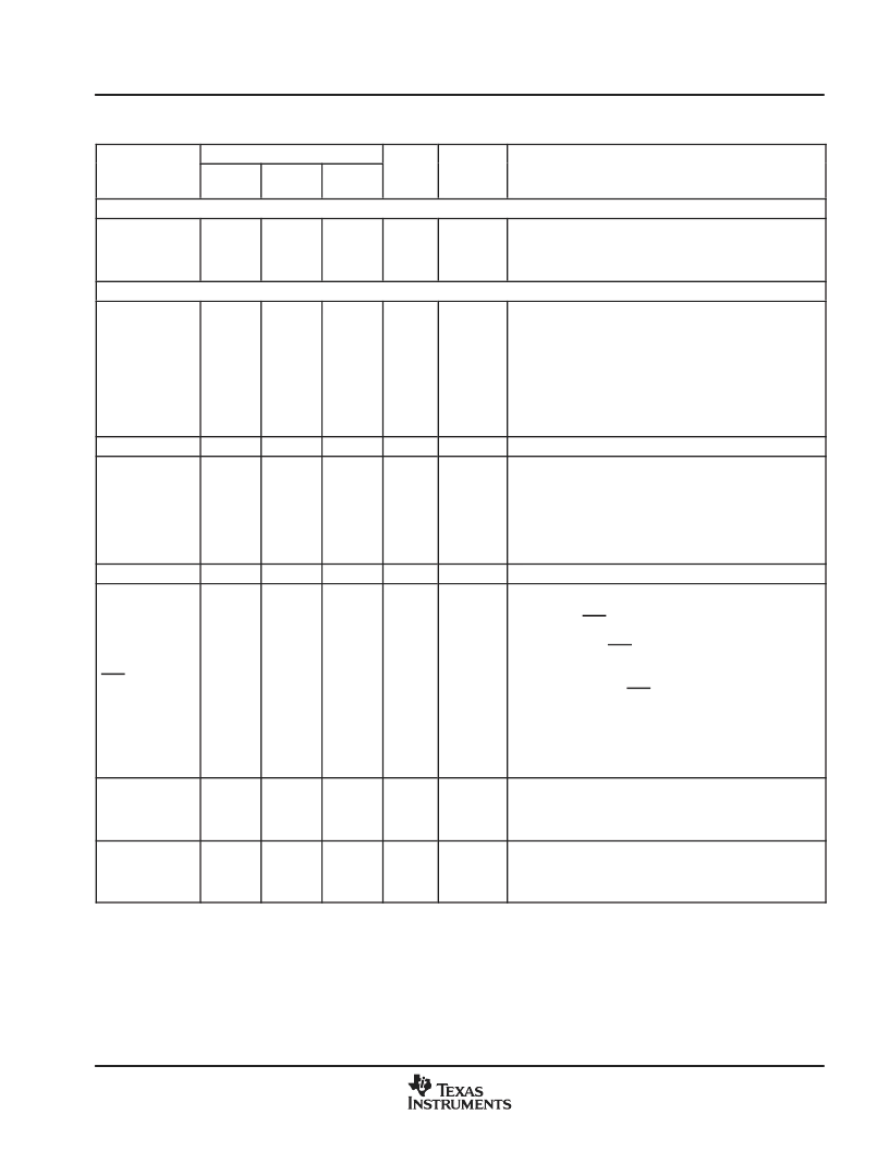
Table 22. Signal Descriptions
(Continued)
NAME
DESCRIPTION
PU/PD§
I/O/Z
PIN NO.
176-PIN
PGF
128-PIN
PBK
179-PIN
GHH
XINTF SIGNALS (2812 ONLY) (CONTINUED)
XREADY
B6
161
I
PU
Ready Signal. Indicates peripheral is ready to complete the
access when asserted to 1. XREADY can be configured to be
a synchronous or an asynchronous input. See the timing
diagrams for more details.
JTAG AND MISCELLANEOUS SIGNALS
X1/XCLKIN
K9
77
58
I
Oscillator Input input to the internal oscillator. This pin is also
used to feed an external clock. The 28x can be operated with
an external clock source, provided that the proper voltage
levels be driven on the X1/XCLKIN pin. It should be noted that
the X1/XCLKIN pin is referenced to the 1.8-V (or 1.9-V) core
digital power supply (VDD), rather than the 3.3-V I/O supply
(VDDIO). A clamping diode may be used to clamp a buffered
clock signal to ensure that the logic-high level does not
exceed VDD (1.8 V or 1.9 V) or a 1.8-V oscillator may be used.
Oscillator Output
X2
M9
76
57
O
XCLKOUT
F11
119
87
O
Output clock derived from SYSCLKOUT to be used for
external wait-state generation and as a general-purpose clock
source. XCLKOUT is either the same frequency, 1/2 the
frequency, or 1/4 the frequency of SYSCLKOUT. At reset,
XCLKOUT = SYSCLKOUT/4. The XCLKOUT signal can be
turned off by setting bit 3 (CLKOFF) of the XINTCNF2 register
to 1.
TESTSEL
A13
134
97
I
PD
Test Pin. Reserved for TI. Must be connected to ground.
XRS
D6
160
113
I/O
PU
Device Reset (in) and Watchdog Reset (out).
Device reset. XRS causes the device to terminate execution.
The PC will point to the address contained at the location
0x3FFFC0. When XRS is brought to a high level, execution
begins at the location pointed to by the PC. This pin is driven
low by the DSP when a watchdog reset occurs. During
watchdog reset, the XRS pin will be driven low for the
watchdog reset duration of 512 XCLKIN cycles.
The output buffer of this pin is an open-drain with an internal
pullup (100
μ
A, typical). It is recommended that this pin be
driven by an open-drain device.
TEST1
M7
67
51
I/O
Test Pin. Reserved for TI. On F281x devices, TEST1 must be
left unconnected. On C281x devices, this pin is a “no connect
(NC)” (i.e., this pin is not connected to any circuitry internal
to the device).
TEST2
N7
66
50
I/O
Test Pin. Reserved for TI. On F281x devices, TEST2 must be
left unconnected. On C281x devices, this pin is a “no connect
(NC)” (i.e., this pin is not connected to any circuitry internal
to the device).
Typical drive strength of the output buffer for all pins is 4 mA except for TDO, XCLKOUT, XF, XINTF, EMU0, and EMU1 pins, which are 8 mA.
I = Input, O = Output, Z = High impedance
§PU = pin has internal pullup; PD = pin has internal pulldown
相關(guān)PDF資料 |
PDF描述 |
|---|---|
| TMS320F2812PGFMEP | Digital Signal Processors |
| TMS320F2810PGFAEP | Digital Signal Processors |
| TMX20F2810PBKAEP | Digital Signal Processors |
| TMS320LC2404APGA | DSP CONTROLLERS |
| TMP320LC2401APAGA | DSP CONTROLLERS |
相關(guān)代理商/技術(shù)參數(shù) |
參數(shù)描述 |
|---|---|
| TMP2681P | 制造商:未知廠家 制造商全稱:未知廠家 功能描述:Telecommunication IC |
| TMP275 | 制造商:BB 制造商全稱:BB 功能描述:0.5∑C Digital Out Temperature Sensor |
| TMP275AID | 功能描述:板上安裝溫度傳感器 0.5C Dig Out Temp Sensor RoHS:否 制造商:Omron Electronics 輸出類型:Digital 配置: 準(zhǔn)確性:+/- 1.5 C, +/- 3 C 溫度閾值: 數(shù)字輸出 - 總線接口:2-Wire, I2C, SMBus 電源電壓-最大:5.5 V 電源電壓-最小:4.5 V 最大工作溫度:+ 50 C 最小工作溫度:0 C 關(guān)閉: 安裝風(fēng)格: 封裝 / 箱體: 設(shè)備功能:Temperature and Humidity Sensor |
| TMP275AID | 制造商:Texas Instruments 功能描述:IC TEMP SENSOR 12BIT |
| TMP275AID | 制造商:Texas Instruments 功能描述:IC DIGITAL TEMP SENSOR |
發(fā)布緊急采購(gòu),3分鐘左右您將得到回復(fù)。