- 您現(xiàn)在的位置:買賣IC網(wǎng) > PDF目錄383876 > T7234A Compliance with the New ETSI PSD Requirement PDF資料下載
參數(shù)資料
| 型號(hào): | T7234A |
| 英文描述: | Compliance with the New ETSI PSD Requirement |
| 中文描述: | 符合新的ETSI PSD的要求 |
| 文件頁數(shù): | 11/116頁 |
| 文件大小: | 1056K |
| 代理商: | T7234A |
第1頁第2頁第3頁第4頁第5頁第6頁第7頁第8頁第9頁第10頁當(dāng)前第11頁第12頁第13頁第14頁第15頁第16頁第17頁第18頁第19頁第20頁第21頁第22頁第23頁第24頁第25頁第26頁第27頁第28頁第29頁第30頁第31頁第32頁第33頁第34頁第35頁第36頁第37頁第38頁第39頁第40頁第41頁第42頁第43頁第44頁第45頁第46頁第47頁第48頁第49頁第50頁第51頁第52頁第53頁第54頁第55頁第56頁第57頁第58頁第59頁第60頁第61頁第62頁第63頁第64頁第65頁第66頁第67頁第68頁第69頁第70頁第71頁第72頁第73頁第74頁第75頁第76頁第77頁第78頁第79頁第80頁第81頁第82頁第83頁第84頁第85頁第86頁第87頁第88頁第89頁第90頁第91頁第92頁第93頁第94頁第95頁第96頁第97頁第98頁第99頁第100頁第101頁第102頁第103頁第104頁第105頁第106頁第107頁第108頁第109頁第110頁第111頁第112頁第113頁第114頁第115頁第116頁
Data Sheet
January 1998
T7256 Single-Chip NT1 (SCNT1) Transceiver
Lucent Technologies Inc.
7
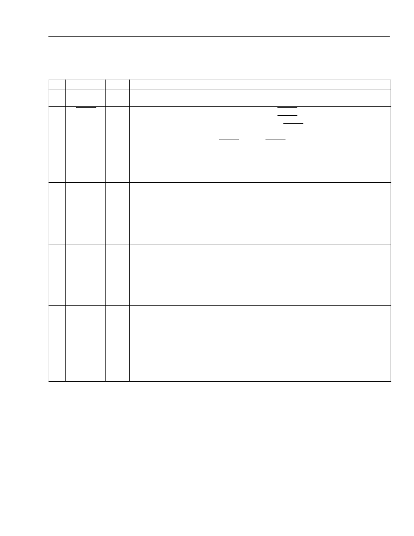
Pin Information
(continued)
Table 1. Pin Descriptions
(continued)
* I
u
= input with internal pull-up; I
d
= input with internal pull-down.
Pin
5,
13
6
Symbol
V
DDD
Type*
—
Name/Function
Digital Power.
5 V
±
5% power supply pins for digital circuitry.
ILOSS
I
u
Insertion Loss Test Control (Active-Low)
transmission for maintenance. The OPTOIN and ILOSS pins should not be used at the
same time (i.e., OPTOIN should be held high when ILOSS is active). This pin would typ-
ically be used if an external ANSI maintenance decoder is being used, in which case
the decoder output drives the ILOSS pin. The ILOSS pin is ignored, and the functionality
is controlled by the ILOSS bit (register CFR0, bit 0) if AUTOCTL = 0 (register GR0, bit
3). Internal 100 k
pull-up resistor on this pin.
0—U transmitter sends SN1 tone continuously.
1—No effect on device operation.
Fixed/Adaptive Timing Mode Select.
If TDMEN = 1 (register GR2, bit 5, default),
selects S/T-interface timing recovery mode:
0—Fixed timing recovery mode.
1—Adaptive timing recovery mode.
TDM Data In.
If TDMEN = 0, this pin is the TDM bus 2B+D data input synchronous with
TDMCLK, and the S/T-interface timing mode is controlled via the FT bit (register GR2,
bit 0). An internal 100 k
pull-up resistor is on this pin.
Power Status #2.
If TDMEN = 1 (register GR2, bit 5, default), this is an input for the
PS2 bit in transmit U-interface data stream. See PS2 bit description (register GR1, bit
1) for PS1 and PS2 message definition. An internal 100 k
pin.
TDM Data Out.
If TDMEN = 0, this pin is the 2.048 MHz TDM bus 2B+D data output
synchronous with TDMCLK, and PS2 is controlled via the PS2 (register GR1, bit 1) mi-
croprocessor register bit.
Power Status #1.
If TDMEN = 1 (register GR2, bit 5, default), this is an input for the
PS1 bit in transmit U-interface data stream. See PS2 bit description (register GR1,
bit 1) for PS1 and PS2 message definition. If PS1E is not driven by an external control
circuit, it must be pulled up externally with a 10 k
ence of primary power. An internal 100 k
pull-down resistor is on this pin.
TDM Clock.
If TDMEN = 0, this pin is the 2.048 MHz TDM clock output synchronous
with U-interface (if active) or is free-running, and PS1 is controlled via the PS1 micro-
processor register bit. TDMCLK will be disabled until at least one of bits 2—7 in register
DFR1 is enabled.
. The ILOSS pin is used to control SN1 tone
7
FTE/
TDMDI
I
u
8
PS2E/
TDMDO
I
d
/O
pull-down resistor is on this
9
PS1E/
TDMCLK
I
d
/O
or less resistor to indicate the pres-
相關(guān)PDF資料 |
PDF描述 |
|---|---|
| T7237A | Compliance with the New ETSI PSD Requirement |
| T7256A | Compliance with the New ETSI PSD Requirement |
| T7288 | CEPT/E1 Line Interface(CEPT/E1 線接口) |
| T7290A | DS1/T1/CEPT/E1 Line Interface(DS1/T1/CEPT/E1 線接口) |
| T7295-1 | E3 Integrated Line Receiver(E3 集成線接收器) |
相關(guān)代理商/技術(shù)參數(shù) |
參數(shù)描述 |
|---|---|
| T7237 | 制造商:未知廠家 制造商全稱:未知廠家 功能描述:Compliance with the New ETSI PSD Requirement |
| T7237A | 制造商:AGERE 制造商全稱:AGERE 功能描述:Compliance with the New ETSI PSD Requirement |
| T7240 | 制造商:TE Connectivity 功能描述: |
| T7-241A5 | 功能描述:撥動(dòng)開關(guān) ON NONE OFF 2 Pole Standard Bat Handle RoHS:否 制造商:OTTO 觸點(diǎn)形式: 開關(guān)功能: 電流額定值: 電壓額定值 AC: 電壓額定值 DC: 功率額定值: 端接類型: 安裝風(fēng)格: 端子密封: 觸點(diǎn)電鍍: 照明: |
| T7-241B1 | 制造商:OTTO 功能描述:Toggle Switches ON NONE ON 2 Pole Standard Bat Handle 制造商:OTTO Engineering Inc 功能描述:Switch Toggle ON None ON DPDT Bat Toggle PC Pins 16A 115VAC 28VDC PC Mount with Threads |
發(fā)布緊急采購,3分鐘左右您將得到回復(fù)。