- 您現(xiàn)在的位置:買賣IC網(wǎng) > PDF目錄384797 > OR4E2 (Lineage Power) Field-Programmable Gate Arrays(現(xiàn)場(chǎng)可編程門陣列) PDF資料下載
參數(shù)資料
| 型號(hào): | OR4E2 |
| 廠商: | Lineage Power |
| 英文描述: | Field-Programmable Gate Arrays(現(xiàn)場(chǎng)可編程門陣列) |
| 中文描述: | 現(xiàn)場(chǎng)可編程門陣列(現(xiàn)場(chǎng)可編程門陣列) |
| 文件頁數(shù): | 33/132頁 |
| 文件大小: | 2667K |
| 代理商: | OR4E2 |
第1頁第2頁第3頁第4頁第5頁第6頁第7頁第8頁第9頁第10頁第11頁第12頁第13頁第14頁第15頁第16頁第17頁第18頁第19頁第20頁第21頁第22頁第23頁第24頁第25頁第26頁第27頁第28頁第29頁第30頁第31頁第32頁當(dāng)前第33頁第34頁第35頁第36頁第37頁第38頁第39頁第40頁第41頁第42頁第43頁第44頁第45頁第46頁第47頁第48頁第49頁第50頁第51頁第52頁第53頁第54頁第55頁第56頁第57頁第58頁第59頁第60頁第61頁第62頁第63頁第64頁第65頁第66頁第67頁第68頁第69頁第70頁第71頁第72頁第73頁第74頁第75頁第76頁第77頁第78頁第79頁第80頁第81頁第82頁第83頁第84頁第85頁第86頁第87頁第88頁第89頁第90頁第91頁第92頁第93頁第94頁第95頁第96頁第97頁第98頁第99頁第100頁第101頁第102頁第103頁第104頁第105頁第106頁第107頁第108頁第109頁第110頁第111頁第112頁第113頁第114頁第115頁第116頁第117頁第118頁第119頁第120頁第121頁第122頁第123頁第124頁第125頁第126頁第127頁第128頁第129頁第130頁第131頁第132頁
Lucent Technologies Inc.
33
Preliminary Data Sheet
August 2000
ORCA Series 4 FPGAs
Programmable Input/Output Cells
(continued)
The PIOs are located along the perimeter of the device.
The PIO name is represented by a two-letter designa-
tion to indicate on which side of the device it is located
followed by a number to indicate in which row or column
it is located. The first letter, P designates that the cell is
a PIO and not a PLC. The second letter indicates the
side of the array where the PIO is located. The four
sides are left (L), right (R), top (T), and bottom (B). The
individual I/O pad is indicated by a single letter (either
A, B, C, or D) placed at the end of the PIO name. As an
example, PL10A indicates a pad located on the left side
of the array in the tenth row.
Each PIC interfaces to four bond pads and contains the
necessary routing resources to provide an interface
between I/O pads and the PLCs. Each PIC is com-
posed of four programmable I/Os and significant routing
resources. Each PIC contains input buffers, output buff-
ers, routing resources, latches/FFs, and logic and can
be configured as an input, output, or bidirectional
I/O. Any PIO is capable of supporting the I/O standard
listed in Table 12 and supporting DDR and ZBTspecifi-
cations.
The I/O on the OR4Exxx Series devices allows compli-
ance with PCI Local Bus (Rev. 2.2) 3.3 V signaling
environments. The signaling environment used for
each input buffer can be selected on a per-pin basis.
The selection provides the appropriate I/O clamping
diodes for PCI compliance.
The CIBs that bound the PIOs have significant local
routing resources, similar to routing in the PLCs. This
new routing increases the ability to fix user pinouts
prior to placement and routing of a design and still
maintain routability. The flexibility provided by the rout-
ing also provides for increased signal speed due to a
greater variety of optimal signal paths.
Included in the PIO routing interface is a fast path from
the input pins to the PFU logic. This feature allows for
input signals to be very quickly processed by the SLIC
decoder function and used on-chip or sent back off of
the FPGA. Also, the Series 4 PIOs include latches and
FFs and options for using fast, dedicated secondary,
and edge clocks.
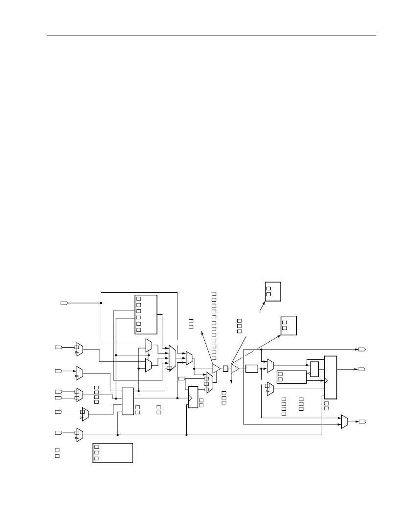
A diagram of a single PIO is shown in Figure 22, and
Table 15 provides an overview of the programmable
functions in an I/O cell.
5-9732(F)
Figure 22. Series 4 PIO Image from ORCAFoundry
OUTSH
OUTDDMUX
OUTDD
OUTFFMUX
OUTFF
CLK4MUX
EC
SC
CE
LSRMUX
LSR
GSR
ENABLED
DISABLED
SRMODE
CE_OVER_LSR
LSR_OVER_CE
ASYNC
CEMUX0
OUTDD
CLK
OUTSH
CLK
OUTDD
OUTREG
OUTREG
DO
CK
SP
LSR
AND
NAND
OR
NOR
XOR
XNOR
PLOGIC
PMUX
OUTSHMUX
BUFMODE
SLEW
FAST
LEVELMODE
LVCMOS18
PCI
SSTL2
SSTL3
HSTL
GTL
GTLPLUS
PECL
LVPECL
LVDS
P2MUX
OUTDD
TSMUX
USRTS
TSREG
DO
CK
LSR
RESET
SET
PULLMODE
UP
DOWN
NONE
INMUX
CEMUXI
NORMAL
INVERTED
LATCHFF
D0
D1
CK
SP
LSR
D0
CK
LATCHFF
LATCH
FF
INDDMUX
INDD
INCK
INFF
RESET
SET
RESET
SET
1
0
0
0
0
1
EC
SC
DELAY
CELL
IOPAD
OUTMUX
CE
1
LVTTL
LVCMOS2
DEL0
DEL1
DEL2
DEL3
DEL0
DEL1
DEL2
DEL3
MILLIAMPS
SIX
TWELVE
TWENTYFOUR
RESISTOR
OFF
ON
KEEPERMODE
OFF
ON
LATCH
FF
相關(guān)PDF資料 |
PDF描述 |
|---|---|
| OR4E4 | Field-Programmable Gate Arrays(現(xiàn)場(chǎng)可編程門陣列) |
| OR4E6 | Field-Programmable Gate Arrays(現(xiàn)場(chǎng)可編程門陣列) |
| ORT4622 | Field-Programmable System Chip (FPSC) Four Channel x 622 Mbits/s Backplane Transceiver(現(xiàn)場(chǎng)可編程系統(tǒng)芯片(四通道x 622 M位/秒背板收發(fā)器)) |
| ORT8850 | Field-Programmable System Chip(現(xiàn)場(chǎng)可編程系統(tǒng)芯片) |
| OS8740230 | Si Optical Receiver, 40 - 870MHz, 225mA max. @ 24VDC |
相關(guān)代理商/技術(shù)參數(shù) |
參數(shù)描述 |
|---|---|
| OR4E2-1BA256 | 制造商:未知廠家 制造商全稱:未知廠家 功能描述:FPGA |
| OR4E2-1BA352 | 制造商:未知廠家 制造商全稱:未知廠家 功能描述:FPGA |
| OR4E2-1BA416 | 制造商:未知廠家 制造商全稱:未知廠家 功能描述:FPGA |
| OR4E2-1BC432 | 制造商:未知廠家 制造商全稱:未知廠家 功能描述:FPGA |
| OR4E2-1BM680 | 制造商:未知廠家 制造商全稱:未知廠家 功能描述:FPGA |
發(fā)布緊急采購,3分鐘左右您將得到回復(fù)。