- 您現(xiàn)在的位置:買賣IC網(wǎng) > PDF目錄384797 > OR4E2 (Lineage Power) Field-Programmable Gate Arrays(現(xiàn)場可編程門陣列) PDF資料下載
參數(shù)資料
| 型號: | OR4E2 |
| 廠商: | Lineage Power |
| 英文描述: | Field-Programmable Gate Arrays(現(xiàn)場可編程門陣列) |
| 中文描述: | 現(xiàn)場可編程門陣列(現(xiàn)場可編程門陣列) |
| 文件頁數(shù): | 16/132頁 |
| 文件大?。?/td> | 2667K |
| 代理商: | OR4E2 |
第1頁第2頁第3頁第4頁第5頁第6頁第7頁第8頁第9頁第10頁第11頁第12頁第13頁第14頁第15頁當(dāng)前第16頁第17頁第18頁第19頁第20頁第21頁第22頁第23頁第24頁第25頁第26頁第27頁第28頁第29頁第30頁第31頁第32頁第33頁第34頁第35頁第36頁第37頁第38頁第39頁第40頁第41頁第42頁第43頁第44頁第45頁第46頁第47頁第48頁第49頁第50頁第51頁第52頁第53頁第54頁第55頁第56頁第57頁第58頁第59頁第60頁第61頁第62頁第63頁第64頁第65頁第66頁第67頁第68頁第69頁第70頁第71頁第72頁第73頁第74頁第75頁第76頁第77頁第78頁第79頁第80頁第81頁第82頁第83頁第84頁第85頁第86頁第87頁第88頁第89頁第90頁第91頁第92頁第93頁第94頁第95頁第96頁第97頁第98頁第99頁第100頁第101頁第102頁第103頁第104頁第105頁第106頁第107頁第108頁第109頁第110頁第111頁第112頁第113頁第114頁第115頁第116頁第117頁第118頁第119頁第120頁第121頁第122頁第123頁第124頁第125頁第126頁第127頁第128頁第129頁第130頁第131頁第132頁
16
Lucent Technologies Inc.
Preliminary Data Sheet
August 2000
ORCA Series 4 FPGAs
Programmable Logic Cells
(continued)
Half-Logic Mode
Series 4 FPGAs are based upon a twin-quad architec-
ture in the PFUs. The byte-wide nature (eight LUTs,
eight latches/FFs) may just as easily be viewed as two
nibbles (two sets of four LUTs, four latches/FFs). The
two nibbles of the PFU are organized so that any nib-
ble-wide feature (excluding some softwired LUT topolo-
gies) can be swapped with any other nibble-wide
feature in another PFU. This provides for very flexible
use of logic and for extremely flexible routing. The half-
logic mode of the PFU takes advantage of the twin-
quad architecture and allows half of a PFU, K
[7:4]
and
associated latches/FFs, to be used in logic mode while
the other half of the PFU, K
[3:0]
and associated
latches/FFs, is used in ripple mode. In half-logic mode,
the ninth FF may be used as a general-purpose FF or
as a register in the ripple mode carry chain.
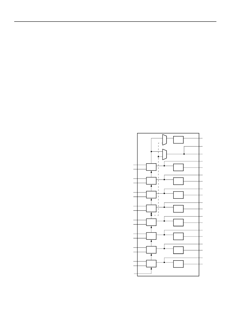
Ripple Mode
The PFU LUTs can be combined to do byte-wide ripple
functions with high-speed carry logic. Each LUT has a
dedicated carry-out net to route the carry to/from any
adjacent LUT. Using the internal carry circuits, fast
arithmetic, counter, and comparison functions can be
implemented in one PFU. Similarly, each PFU has
carry-in (CIN, FCIN) and carry-out (COUT, FCOUT)
ports for fast-carry routing between adjacent PFUs.
The ripple mode is generally used in operations on two
data buses. A single PFU can support an 8-bit ripple
function. Data buses of 4 bits and less can use the
nibble-wide ripple chain that is available in half-logic
mode. This nibble-wide ripple chain is also useful for
longer ripple chains where the length modulo 8 is four
or less. For example, a 12-bit adder (12 modulo 8 = 4)
can be implemented in one PFU in ripple mode (8 bits)
and one PFU in half-logic mode (4 bits), freeing half of
a PFU for general logic mode functions.
Each LUT has two operands and a ripple (generally
carry) input, and provides a result and ripple (generally
carry) output. A single bit is rippled from the previous
LUT and is used as input into the current LUT. For LUT
K
0
, the ripple input is from the PFU CIN or FCIN port.
The CIN/FCIN data can come from either the fast-carry
routing (FCIN) or the PFU input (CIN), or it can be tied
to logic 1 or logic 0.
In the following discussions, the notations LUT K
7
/K
3
and F[7:0]/F[3:0]
are used to denote the LUT that pro-
vides the carry-out and the data outputs for full PFU
ripple operation (K
7
, F[7:0]) and half-logic ripple
operation (K
3
, F[3:0]), respectively. The ripple mode
diagram (Figure 9) shows full PFU ripple operation,
with half-logic ripple connections shown as dashed
lines.
The result output and ripple output are calculated by
using generate/propagate circuitry. In ripple mode, the
two operands are input into K
Z
[1] and K
Z
[0] of each
LUT. The result bits, one per LUT, are F[7:0]/F[3:0]
(see
Figure 9). The ripple output from LUT K
7
/K
3
can be
routed on dedicated carry circuitry into any of four adja-
cent PLCs, and it can be placed on the PFU COUT/
FCOUT outputs. This allows the PLCs to be cascaded
in the ripple mode so that nibble-wide ripple functions
can be expanded easily to any length.
Result outputs and the carry-out may optionally be reg-
istered within the PFU. The capability to register the
ripple results, including the carry output, provides for
improved counter performance and simplified pipelin-
ing in arithmetic functions.
5-5755(F).
Figure 9. Ripple Mode
F7
K
7
[1]
K
7
[0]
K7
D
Q
C
C
D
Q
Q7
REGOUT
COUT
F6
K
6
[1]
K
6
[0]
K6
D
Q
Q6
F4
K
4
[1]
K
4
[0]
K4
D
Q
Q4
F3
K
3
[1]
K
3
[0]
K3
D
Q
Q3
F2
K
2
[1]
K
2
[0]
K2
D
Q
Q2
F1
K
1
[1]
K
1
[0]
K1
D
Q
Q1
F5
K
5
[1]
K
5
[0]
K5
D
Q
Q5
F0
K
0
[1]
K
0
[0]
K0
D
Q
Q0
CIN/FCIN
FCOUT
相關(guān)PDF資料 |
PDF描述 |
|---|---|
| OR4E4 | Field-Programmable Gate Arrays(現(xiàn)場可編程門陣列) |
| OR4E6 | Field-Programmable Gate Arrays(現(xiàn)場可編程門陣列) |
| ORT4622 | Field-Programmable System Chip (FPSC) Four Channel x 622 Mbits/s Backplane Transceiver(現(xiàn)場可編程系統(tǒng)芯片(四通道x 622 M位/秒背板收發(fā)器)) |
| ORT8850 | Field-Programmable System Chip(現(xiàn)場可編程系統(tǒng)芯片) |
| OS8740230 | Si Optical Receiver, 40 - 870MHz, 225mA max. @ 24VDC |
相關(guān)代理商/技術(shù)參數(shù) |
參數(shù)描述 |
|---|---|
| OR4E2-1BA256 | 制造商:未知廠家 制造商全稱:未知廠家 功能描述:FPGA |
| OR4E2-1BA352 | 制造商:未知廠家 制造商全稱:未知廠家 功能描述:FPGA |
| OR4E2-1BA416 | 制造商:未知廠家 制造商全稱:未知廠家 功能描述:FPGA |
| OR4E2-1BC432 | 制造商:未知廠家 制造商全稱:未知廠家 功能描述:FPGA |
| OR4E2-1BM680 | 制造商:未知廠家 制造商全稱:未知廠家 功能描述:FPGA |
發(fā)布緊急采購,3分鐘左右您將得到回復(fù)。