- 您現(xiàn)在的位置:買(mǎi)賣(mài)IC網(wǎng) > PDF目錄360517 > 7560 7560 Group Datasheet Datasheet 1682K/JAN.14.03 PDF資料下載
參數(shù)資料
| 型號(hào): | 7560 |
| 英文描述: | 7560 Group Datasheet Datasheet 1682K/JAN.14.03 |
| 中文描述: | 7560組數(shù)據(jù)表數(shù)據(jù)表1682K/JAN.14.03 |
| 文件頁(yè)數(shù): | 41/90頁(yè) |
| 文件大?。?/td> | 1682K |
| 代理商: | 7560 |
第1頁(yè)第2頁(yè)第3頁(yè)第4頁(yè)第5頁(yè)第6頁(yè)第7頁(yè)第8頁(yè)第9頁(yè)第10頁(yè)第11頁(yè)第12頁(yè)第13頁(yè)第14頁(yè)第15頁(yè)第16頁(yè)第17頁(yè)第18頁(yè)第19頁(yè)第20頁(yè)第21頁(yè)第22頁(yè)第23頁(yè)第24頁(yè)第25頁(yè)第26頁(yè)第27頁(yè)第28頁(yè)第29頁(yè)第30頁(yè)第31頁(yè)第32頁(yè)第33頁(yè)第34頁(yè)第35頁(yè)第36頁(yè)第37頁(yè)第38頁(yè)第39頁(yè)第40頁(yè)當(dāng)前第41頁(yè)第42頁(yè)第43頁(yè)第44頁(yè)第45頁(yè)第46頁(yè)第47頁(yè)第48頁(yè)第49頁(yè)第50頁(yè)第51頁(yè)第52頁(yè)第53頁(yè)第54頁(yè)第55頁(yè)第56頁(yè)第57頁(yè)第58頁(yè)第59頁(yè)第60頁(yè)第61頁(yè)第62頁(yè)第63頁(yè)第64頁(yè)第65頁(yè)第66頁(yè)第67頁(yè)第68頁(yè)第69頁(yè)第70頁(yè)第71頁(yè)第72頁(yè)第73頁(yè)第74頁(yè)第75頁(yè)第76頁(yè)第77頁(yè)第78頁(yè)第79頁(yè)第80頁(yè)第81頁(yè)第82頁(yè)第83頁(yè)第84頁(yè)第85頁(yè)第86頁(yè)第87頁(yè)第88頁(yè)第89頁(yè)第90頁(yè)
SINGLE-CHIP 8-BIT CMOS MICROCOMPUTER
MITSUBISHI MICROCOMPUTERS
7560 Group
40
A-D CONVERTER
[A-D Conversion Low-Order Register (ADL)]
0014
16
[A-D Conversion High-Order Register (ADH)]
0035
16
The A-D conversion registers are read-only registers that store the
result of an A-D conversion . When reading this register during an
A-D conversion, the previous conversion result is read.
The high-order 8 bits of a conversion result is stored in the A-D
conversion high-order register (address 0035
16
), and the low-or-
der 2 bits of the same result are stored in bit 7 and bit 6 of the A-D
conversion low-order register (address 0014
16
).
Bit 0 of the A-D conversion low-order register is the conversion
mode selection bit. When this bit is set to
“
0
”
, that becomes the
10-bit A-D mode. When this bit is set to
“
1
”
, that becomes the 8-bit
A-D mode.
[A-D Control Register (ADCON)] 0034
16
The A-D control register controls the A-D conversion process. Bits
0 to 2 of this register select specific analog input pins. Bit 3 indi-
cates the completion of an A-D conversion. The value of this bit re-
mains at
“
0
”
during an A-D conversion, then it is set to
“
1
”
when
the A-D conversion is completed. Writing
“
0
”
to this bit starts the
A-D conversion.
Bit 4 is the V
REF
input switch bit which controls connection of the
resistor ladder and the reference voltage input pin (V
REF
). The
resistor ladder is always connected to V
REF
when bit 4 is set to
“
1
”
. When bit 4 is set to
“
0
”
, the resistor ladder is cut off from V
REF
except for A-D conversion performed. When bit 5, which is the AD
external trigger valid bit, is set to
“
1
”
, A-D conversion starts also by
a falling edge of an ADT input. When using an A-D external trigger,
set the P5
7
/ADT pin to input mode (set
“
0
”
to bit 7 of port P5 direc-
tion register).
Comparison Voltage Generator
The comparison voltage generator divides the voltage between
AV
SS
and V
REF
by 256 (when 8-bit A-D mode) or 1024 (when 10-
bit A-D mode), and outputs the divided voltages.
Channel Selector
The channel selector selects one of the input ports P6
7
/AN
7
–
P6
0
/AN
0
.
Comparator and Control Circuit
The comparator and control circuit compare an analog input volt-
age with the comparison voltage and store the result in the A-D
conversion register. When an A-D conversion is completed, the
control circuit sets the AD conversion completion bit and the AD
converter interrupt request bit to
“
1
”
.
Note that because the comparator consists of a capacitor
coupling, set f(X
IN
) to 500 kHz or more during an A-D conversion.
Use the clock divided from the main clock f(X
IN
) as the system clock
φ
.
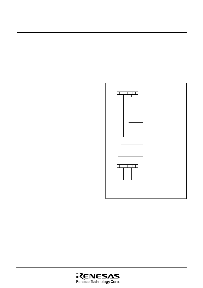
Fig. 40 Structure of A-D converter-related registers
A
(
A
-
D
D
C
Analog input pin selection bits
b2b1b0
0 0 0 : P6
0
/AN
0
0 0 1 : P6
1
/AN
1
0 1 0 : P6
2
/AN
2
0 1 1 : P6
3
/AN
3
1 0 0 : P6
4
/AN
4
1 0 1 : P6
5
/AN
5
1 1 0 : P6
6
/AN
6
1 1 1 : P6
7
/AN
7
c
o
O
n
N
t
r
o
:
l
a
r
d
e
g
r
i
e
s
t
e
s
r
d
s
0
0
3
4
1
6
)
AD conversion completion bit
0 : Conversion in progress
1 : Conversion completed
V
R
E
i
n
p
u
t
s
w
i
t
0
:
A
U
T
O
1
:
O
N
AD external trigger valid bit
0 : A-D external trigger invalid
1 : A-D external trigger valid
Interrupt source selection bit
0 : Interrupt request at A-D
conversion completed
1 : Interrupt request at ADT
input falling
Not used (
“
0
”
at reading)
F
c
h
b
i
t
b7
b0
A
(
A
-
D
D
L
c
o
:
Conversion mode selection bit
0 : 10-bit A-D mode
1 : 8-bit A-D mode
n
a
v
d
e
d
r
r
s
e
i
o
s
n
s
l
o
0
w
1
-
4
1
o
r
6
)
d
e
r
r
e
g
i
s
t
e
r
0
Not used (
“
0
”
at reading)
For
10-bit A-D mode
A-D conversion result
For
8-bit A-D mode
Not used (undefined at reading)
b7
b0
相關(guān)PDF資料 |
PDF描述 |
|---|---|
| 7561Z0001S13 | READER PANEL MOUNT |
| 7561Z0001S13LF | READER PANEL MOUNT |
| 7561Z0001S14 | READER PANEL MOUNT |
| 7561Z0001S14LF | READER PANEL MOUNT |
| 7561Z0001S15 | READER PANEL MOUNT |
相關(guān)代理商/技術(shù)參數(shù) |
參數(shù)描述 |
|---|---|
| 7560 6 43 01 D | 制造商:Hummel 功能描述:Bulk |
| 7560 6 51 01 D | 制造商:Hummel 功能描述: |
| 7560_03 | 制造商:RENESAS 制造商全稱(chēng):Renesas Technology Corp 功能描述:SINGLE-CHIP 8-BIT CMOS MICROCOMPUTER |
| 7560_0308 | 制造商:RENESAS 制造商全稱(chēng):Renesas Technology Corp 功能描述:Difference among various products |
| 7-5-600 | 功能描述:3M 600 SCOTCH TRANSPARENT FILM T 制造商:3m (tc) 系列:600 零件狀態(tài):在售 標(biāo)準(zhǔn)包裝:1 |
發(fā)布緊急采購(gòu),3分鐘左右您將得到回復(fù)。