- 您現(xiàn)在的位置:買(mǎi)賣(mài)IC網(wǎng) > PDF目錄360517 > 7560 7560 Group Datasheet Datasheet 1682K/JAN.14.03 PDF資料下載
參數(shù)資料
| 型號(hào): | 7560 |
| 英文描述: | 7560 Group Datasheet Datasheet 1682K/JAN.14.03 |
| 中文描述: | 7560組數(shù)據(jù)表數(shù)據(jù)表1682K/JAN.14.03 |
| 文件頁(yè)數(shù): | 33/90頁(yè) |
| 文件大小: | 1682K |
| 代理商: | 7560 |
第1頁(yè)第2頁(yè)第3頁(yè)第4頁(yè)第5頁(yè)第6頁(yè)第7頁(yè)第8頁(yè)第9頁(yè)第10頁(yè)第11頁(yè)第12頁(yè)第13頁(yè)第14頁(yè)第15頁(yè)第16頁(yè)第17頁(yè)第18頁(yè)第19頁(yè)第20頁(yè)第21頁(yè)第22頁(yè)第23頁(yè)第24頁(yè)第25頁(yè)第26頁(yè)第27頁(yè)第28頁(yè)第29頁(yè)第30頁(yè)第31頁(yè)第32頁(yè)當(dāng)前第33頁(yè)第34頁(yè)第35頁(yè)第36頁(yè)第37頁(yè)第38頁(yè)第39頁(yè)第40頁(yè)第41頁(yè)第42頁(yè)第43頁(yè)第44頁(yè)第45頁(yè)第46頁(yè)第47頁(yè)第48頁(yè)第49頁(yè)第50頁(yè)第51頁(yè)第52頁(yè)第53頁(yè)第54頁(yè)第55頁(yè)第56頁(yè)第57頁(yè)第58頁(yè)第59頁(yè)第60頁(yè)第61頁(yè)第62頁(yè)第63頁(yè)第64頁(yè)第65頁(yè)第66頁(yè)第67頁(yè)第68頁(yè)第69頁(yè)第70頁(yè)第71頁(yè)第72頁(yè)第73頁(yè)第74頁(yè)第75頁(yè)第76頁(yè)第77頁(yè)第78頁(yè)第79頁(yè)第80頁(yè)第81頁(yè)第82頁(yè)第83頁(yè)第84頁(yè)第85頁(yè)第86頁(yè)第87頁(yè)第88頁(yè)第89頁(yè)第90頁(yè)
SINGLE-CHIP 8-BIT CMOS MICROCOMPUTER
MITSUBISHI MICROCOMPUTERS
7560 Group
32
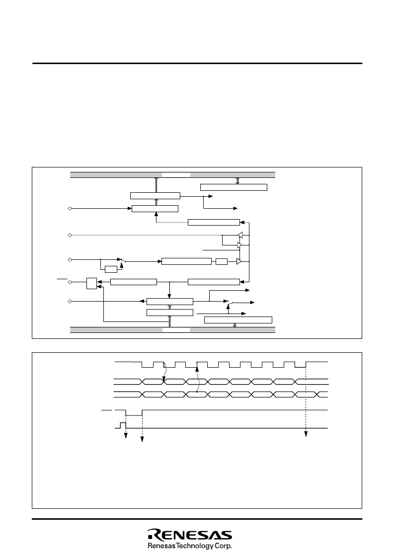
SERIAL I/O
Serial I/O1
Serial I/O1 can be used as either clock synchronous or asynchro-
nous (UART) serial I/O. A dedicated timer (baud rate generator) is
also provided for baud rate generation.
(1) Clock Synchronous Serial I/O Mode
Clock synchronous serial I/O mode is selected by setting the se-
rial I/O1 mode selection bit of the serial I/O1 control register to
“
1
”
.
For clock synchronous serial I/O mode, the transmitter and the re-
ceiver must use the same clock as an operation clock.
When an internal clock is selected as an operation clock, transmit
or receive is started by a write signal to the transmit buffer regis-
ter.
When an external clock is selected as an operation clock, serial I/
O1 becomes the state where transmit or receive can be performed
by a write signal to the transmit buffer register. Transmit and re-
ceive are started by input of an external clock.
Fig. 28 Block diagram of clock synchronous serial I/O1
Fig. 29 Operation of clock synchronous serial I/O1 function
P
4
6
/
S
C
L
K
1
P
4
7
/
S
R
D
Y
1
P
4
4
/
R
X
D
P4
5
/T
X
D
X
I
N
1
/
4
1/4
F
/
F
Serial I/O1 status register
Serial I/O1 control register
R
e
c
e
i
v
e
b
u
f
f
e
r
r
e
g
i
s
t
e
r
A
d
d
r
e
s
s
0
0
1
8
1
6
Receive shift register
Receive buffer full flag (RBF)
R
e
c
e
i
v
e
i
n
t
e
r
r
u
p
t
r
e
q
u
e
s
t
Receive clock control circuit
S
h
i
f
t
c
l
o
c
k
Serial I/O1 synchronous
clock selection bit
Frequency division ratio 1/(n+1)
Baud rate generator
A
d
d
r
e
s
s
0
0
1
C
1
6
BRG count source selection bit
F
a
l
l
i
n
g
-
e
d
g
e
d
e
t
e
c
t
o
r
Data bus
Address 0018
16
S
h
i
f
t
c
l
o
c
k
Transmit shift register shift completion flag (TSC)
Transmit interrupt source selection bit
Transmit buffer empty flag (TBE)
Address 0019
16
T
r
a
n
s
m
i
t
i
n
t
e
r
r
u
p
t
r
e
q
u
e
s
t
Data bus
A
d
d
r
e
s
s
0
0
1
A
1
6
T
r
a
n
s
m
i
t
b
u
f
f
e
r
r
e
g
i
s
t
e
r
T
r
a
n
s
m
i
t
s
h
i
f
t
r
e
g
i
s
t
e
r
T
r
a
n
s
m
i
t
cl
o
c
k
c
o
n
t
r
o
l
c
i
r
c
u
i
t
Receive enable signal S
RDY1
D
7
D
0
D
1
D
2
D
3
D
4
D
5
D
6
RBF =
“
1
”
TSC =
“
1
”
v
e
r
r
u
d
e
t
e
c
t
TBE =
“
0
”
TBE =
“
1
”
TSC =
“
0
”
T
(
c
r
1
a
/
2
o
n
c
s
t
k
m
o
,
o
i
t
/
2
a
a
n
0
n
d
4
e
r
x
e
o
t
e
c
f
e
t
r
n
i
v
e
a
e
l
i
c
s
n
l
h
t
e
o
i
f
r
k
t
n
c
a
)
l
l
o
c
k
1
8
h
l
r
c
S
e
r
i
a
l
o
u
t
p
u
t
T
X
D
S
e
r
i
a
l
i
n
p
u
t
R
X
D
W
b
r
i
f
t
e
e
r
s
r
i
e
g
n
g
a
i
s
l
t
e
t
o
r
r
(
e
a
c
d
e
d
i
r
v
e
e
s
/
s
t
r
a
0
n
0
s
1
m
8
1
i
6
)
t
u
f
O
n
o
n
e
r
r
o
r
(
O
E
)
i
N
o
t
e
s 1
2
:
A
I
f
b
S
a
I
:
T
f
e
e
f
/
O
h
t
d
e
a
o
l
e
e
1
e
r
a
u
c
r
s
d
a
i
p
t
h
c
o
e
t
a
t
e
t
t
a
t
r
r
o
s
a
o
I
a
i
t
n
t
e
n
e
r
n
s
l
r
/
O
s
n
i
n
i
a
m
e
g
1
f
e
t
u
l
i
i
s
r
e
r
o
o
I
/
t
t
c
r
u
O
s
e
e
i
t
n
h
s
1
h
r
i
g
e
l
i
f
.
v
,
y
t
t
t
r
o
t
r
f
a
h
a
r
n
p
e
n
o
s
e
T
s
m
m
r
a
x
D
i
t
h
i
t
t
i
o
p
b
T
X
D
n
t
e
n
h
i
u
n
f
f
k
e
e
r
p
u
p
s
e
r
p
e
i
n
t
e
n
s
g
.
r
e
d
i
D
7
s
t
e
o
r
u
w
t
h
p
u
n
t
v
T
a
S
l
u
C
e
.
=
:
t
s
u
h
e
n
r
i
w
m
t
e
“
0
”
,
t
h
e
t
r
a
n
s
m
i
t
c
l
o
c
k
i
s
g
e
n
e
r
a
t
e
d
c
o
n
t
i
n
u
o
u
s
l
y
a
n
d
s
e
r
i
a
l
d
a
t
a
c
a
n
t
t
t
c
r
r
l
t
e
i
3
:
r
a
r
q
e
u
d
e
(
s
T
t
S
f
C
a
c
t
o
r
1
b
”
e
)
,
t
w
b
e
e
s
n
e
w
t
i
h
g
e
n
t
h
t
e
h
e
t
r
a
t
r
n
a
s
n
m
s
m
i
t
i
n
t
b
t
e
u
r
f
r
f
u
e
p
r
t
r
e
s
g
o
i
s
r
t
c
e
e
r
h
s
a
e
s
l
e
c
e
m
t
i
o
p
n
t
i
b
e
d
t
(
(
T
T
I
B
C
E
)
o
=
f
“
t
1
h
”
e
)
s
o
r
r
t
=
“
y
t
n
i
u
i
e
i
a
l
4
e
i
n
t
e
r
r
u
p
t
r
e
q
u
e
s
t
o
c
c
u
r
s
w
h
e
n
t
h
e
r
e
c
e
i
v
e
b
u
f
f
e
r
f
u
l
l
f
l
a
g
(
R
B
F
)
b
e
c
o
m
e
s
“
1
”
.
D
7
D
0
D
1
D
2
D
3
D
4
D
5
D
6
(N
o
t
e
1
)
(Note 3)
(Note 2)
(Note 3)
(Note 4)
相關(guān)PDF資料 |
PDF描述 |
|---|---|
| 7561Z0001S13 | READER PANEL MOUNT |
| 7561Z0001S13LF | READER PANEL MOUNT |
| 7561Z0001S14 | READER PANEL MOUNT |
| 7561Z0001S14LF | READER PANEL MOUNT |
| 7561Z0001S15 | READER PANEL MOUNT |
相關(guān)代理商/技術(shù)參數(shù) |
參數(shù)描述 |
|---|---|
| 7560 6 43 01 D | 制造商:Hummel 功能描述:Bulk |
| 7560 6 51 01 D | 制造商:Hummel 功能描述: |
| 7560_03 | 制造商:RENESAS 制造商全稱(chēng):Renesas Technology Corp 功能描述:SINGLE-CHIP 8-BIT CMOS MICROCOMPUTER |
| 7560_0308 | 制造商:RENESAS 制造商全稱(chēng):Renesas Technology Corp 功能描述:Difference among various products |
| 7-5-600 | 功能描述:3M 600 SCOTCH TRANSPARENT FILM T 制造商:3m (tc) 系列:600 零件狀態(tài):在售 標(biāo)準(zhǔn)包裝:1 |
發(fā)布緊急采購(gòu),3分鐘左右您將得到回復(fù)。