- 您現(xiàn)在的位置:買賣IC網(wǎng) > PDF目錄360517 > 7560 7560 Group Datasheet Datasheet 1682K/JAN.14.03 PDF資料下載
參數(shù)資料
| 型號: | 7560 |
| 英文描述: | 7560 Group Datasheet Datasheet 1682K/JAN.14.03 |
| 中文描述: | 7560組數(shù)據(jù)表數(shù)據(jù)表1682K/JAN.14.03 |
| 文件頁數(shù): | 30/90頁 |
| 文件大小: | 1682K |
| 代理商: | 7560 |
第1頁第2頁第3頁第4頁第5頁第6頁第7頁第8頁第9頁第10頁第11頁第12頁第13頁第14頁第15頁第16頁第17頁第18頁第19頁第20頁第21頁第22頁第23頁第24頁第25頁第26頁第27頁第28頁第29頁當(dāng)前第30頁第31頁第32頁第33頁第34頁第35頁第36頁第37頁第38頁第39頁第40頁第41頁第42頁第43頁第44頁第45頁第46頁第47頁第48頁第49頁第50頁第51頁第52頁第53頁第54頁第55頁第56頁第57頁第58頁第59頁第60頁第61頁第62頁第63頁第64頁第65頁第66頁第67頁第68頁第69頁第70頁第71頁第72頁第73頁第74頁第75頁第76頁第77頁第78頁第79頁第80頁第81頁第82頁第83頁第84頁第85頁第86頁第87頁第88頁第89頁第90頁
SINGLE-CHIP 8-BIT CMOS MICROCOMPUTER
MITSUBISHI MICROCOMPUTERS
7560 Group
29
Timer X
Timer X is a 16-bit timer and is equipped with the timer latch. The
division ratio of timer X is given by 1/(n+1), where n is the value in
the timer latch. Timer X is a down-counter. When the contents of
timer X reach
“
0000
16
”
, an underflow occurs at the next count
pulse and the contents of the timer latch are reloaded into the
timer and the count is continued. When the timer underflows, the
timer X interrupt request bit is set to
“
1
”
.
Timer X can be selected in one of four modes by the timer X mode
register and can be controlled the timer X write and the real time
port.
(1) Timer mode
The timer counts f(X
IN
)/16 (or f(X
CIN
)/16 in low-speed mode).
(2) Pulse output mode
Each time the timer underflows, a signal output from the CNTR
0
pin is inverted. Except for this, the operation in pulse output mode
is the same as in timer mode. When using a timer in this mode,
set the P5
4
/CNTR
0
pin to output mode (set
“
1
”
to bit 4 of port P5
direction register).
(3) Event counter mode
The timer counts signals input through the CNTR
0
pin.
Except for this, the operation in event counter mode is the same
as in timer mode. When using a timer in this mode, set the P5
4
/
CNTR
0
pin to input mode (set
“
0
”
to bit 4 of port P5 direction reg-
ister).
(4) Pulse width measurement mode
The count source is f(X
IN
)/16 (or f(X
CIN
)/16 in low-speed mode). If
CNTR
0
active edge switch bit is
“
0
”
, the timer counts while the
input signal of CNTR
0
pin is at
“
H
”
. If it is
“
1
”
, the timer counts
while the input signal of CNTR
0
pin is at
“
L
”
. When using a timer in
this mode, set the P5
4
/CNTR
0
pin to input mode (set
“
0
”
to bit 4 of
port P5 direction register).
G
Read and write to timer X high-order, low-order registers
When reading and writing to the timer X high-order and low-order
registers, be sure to read/write both the timer X high- and low-or-
der registers.
When reading the timer X high-order and low-order registers, read
the high-order register first. When writing to the timer X high-order
and low-order registers, write the low-order register first. The timer
X cannot perform the correct operation if the next operation is per-
formed.
Write operation to the high- or low-order register before reading
the timer X low-order register
Read operation from the high- or low-order register before writing
to the timer X high-order register
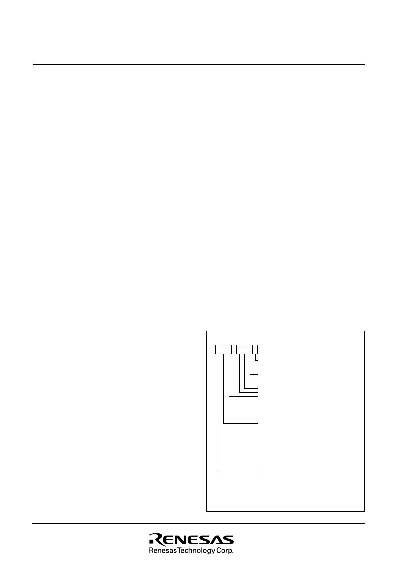
Fig. 25 Structure of timer X mode register
T
(
i
T
m
e
M
r
X
:
m
d
o
d
d
r
e
e
s
s
r
e
0
g
0
i
s
2
t
7
1
e
r
X
a
6
)
Timer X write control bit
0 : Write value in latch and timer
1 : Write value in latch only
Real time port control bit
0 : Real time port function invalid
1 : Real time port function valid
RTP
0
data for real time port
RTP
1
data for real time port
Timer X operating mode bits
b5 b4
0
0 : Timer mode
0
1 : Pulse output mode
1
0 : Event counter mode
1
1 : Pulse width measurement mode
CNTR
0
active edge switch bit
0 : Count at rising edge in event counter mode
Start from
“
H
”
output in pulse output mode
Measure
“
H
”
pulse width in pulse width measurement
mode
Falling edge active for CNTR
0
interrupt
1 : Count at falling edge in event counter mode
Start from
“
L
”
output in pulse output mode
Measure
“
L
”
pulse width in pulse width measurement
mode
Rising edge active for CNTR
0
interrupt
Timer X stop control bit
0 : Count start
1 : Count stop
b7
b0
G
Timer X Write Control
Which write control can be selected by the timer X write control bit
(bit 0) of the timer X mode register (address 0027
16
), writing data
to both the latch and the timer at the same time or writing data
only to the latch. When the operation
“
writing data only to the
latch
”
is selected, the value is set to the timer latch by writing data
to the timer X register and the timer is updated at next underflow.
After reset, the operation
“
writing data to both the latch and the
timer at the same time
”
is selected, and the value is set to both
the latch and the timer at the same time by writing data to the
timer X register. The write operation is independent of timer X
count operation, operating or stopping.
When the value is written in latch only, a value is simultaneously
set to the timer X and the timer X latch if the writing in the high-
order register and the underflow of timer X are performed at the
same timing. Unexpected value may be set in the high-order timer
on this occasion.
G
Real Time Port Control
While the real time port function is valid, data for the real time port
are output from ports P5
2
and P5
3
each time the timer X
underflows. (However, if the real time port control bit is changed
from
“
0
”
to
“
1
”
after set of the real time port data, data are output
independent of the timer X operation.) If the data for the real time
port is changed while the real time port function is valid, the
changed data are output at the next underflow of timer X.
Before using this function, set the P5
2
/RTP
0
, P5
3
/RTP
1
pins to
output mode (set
“
1
”
to bits 2, 3 of port P5 direction register).
I
Note on CNTR
0
interrupt active edge selection
CNTR
0
interrupt active edge depends on the CNTR
0
active edge
switch bit.
相關(guān)PDF資料 |
PDF描述 |
|---|---|
| 7561Z0001S13 | READER PANEL MOUNT |
| 7561Z0001S13LF | READER PANEL MOUNT |
| 7561Z0001S14 | READER PANEL MOUNT |
| 7561Z0001S14LF | READER PANEL MOUNT |
| 7561Z0001S15 | READER PANEL MOUNT |
相關(guān)代理商/技術(shù)參數(shù) |
參數(shù)描述 |
|---|---|
| 7560 6 43 01 D | 制造商:Hummel 功能描述:Bulk |
| 7560 6 51 01 D | 制造商:Hummel 功能描述: |
| 7560_03 | 制造商:RENESAS 制造商全稱:Renesas Technology Corp 功能描述:SINGLE-CHIP 8-BIT CMOS MICROCOMPUTER |
| 7560_0308 | 制造商:RENESAS 制造商全稱:Renesas Technology Corp 功能描述:Difference among various products |
| 7-5-600 | 功能描述:3M 600 SCOTCH TRANSPARENT FILM T 制造商:3m (tc) 系列:600 零件狀態(tài):在售 標(biāo)準(zhǔn)包裝:1 |
發(fā)布緊急采購,3分鐘左右您將得到回復(fù)。