- 您現(xiàn)在的位置:買賣IC網(wǎng) > PDF目錄384024 > TMX320DM6446ZWT (Texas Instruments, Inc.) Digital Media System on-Chip PDF資料下載
參數(shù)資料
| 型號(hào): | TMX320DM6446ZWT |
| 廠商: | Texas Instruments, Inc. |
| 英文描述: | Digital Media System on-Chip |
| 中文描述: | 數(shù)字媒體系統(tǒng)芯片 |
| 文件頁數(shù): | 127/214頁 |
| 文件大小: | 1699K |
| 代理商: | TMX320DM6446ZWT |
第1頁第2頁第3頁第4頁第5頁第6頁第7頁第8頁第9頁第10頁第11頁第12頁第13頁第14頁第15頁第16頁第17頁第18頁第19頁第20頁第21頁第22頁第23頁第24頁第25頁第26頁第27頁第28頁第29頁第30頁第31頁第32頁第33頁第34頁第35頁第36頁第37頁第38頁第39頁第40頁第41頁第42頁第43頁第44頁第45頁第46頁第47頁第48頁第49頁第50頁第51頁第52頁第53頁第54頁第55頁第56頁第57頁第58頁第59頁第60頁第61頁第62頁第63頁第64頁第65頁第66頁第67頁第68頁第69頁第70頁第71頁第72頁第73頁第74頁第75頁第76頁第77頁第78頁第79頁第80頁第81頁第82頁第83頁第84頁第85頁第86頁第87頁第88頁第89頁第90頁第91頁第92頁第93頁第94頁第95頁第96頁第97頁第98頁第99頁第100頁第101頁第102頁第103頁第104頁第105頁第106頁第107頁第108頁第109頁第110頁第111頁第112頁第113頁第114頁第115頁第116頁第117頁第118頁第119頁第120頁第121頁第122頁第123頁第124頁第125頁第126頁當(dāng)前第127頁第128頁第129頁第130頁第131頁第132頁第133頁第134頁第135頁第136頁第137頁第138頁第139頁第140頁第141頁第142頁第143頁第144頁第145頁第146頁第147頁第148頁第149頁第150頁第151頁第152頁第153頁第154頁第155頁第156頁第157頁第158頁第159頁第160頁第161頁第162頁第163頁第164頁第165頁第166頁第167頁第168頁第169頁第170頁第171頁第172頁第173頁第174頁第175頁第176頁第177頁第178頁第179頁第180頁第181頁第182頁第183頁第184頁第185頁第186頁第187頁第188頁第189頁第190頁第191頁第192頁第193頁第194頁第195頁第196頁第197頁第198頁第199頁第200頁第201頁第202頁第203頁第204頁第205頁第206頁第207頁第208頁第209頁第210頁第211頁第212頁第213頁第214頁
www.ti.com
P
TMS320DM6446
Digital Media System on-Chip
SPRS283–DECEMBER 2005
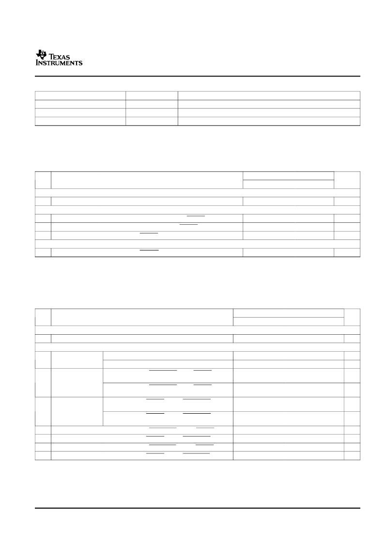
Table 5-29. EMIFA/NAND Registers (continued)
HEX ADDRESS RANGE
0x01E0 0078
0x01E0 007C
0x01E0 0080 - 0x01E0 0FFF
ACRONYM
NANDF3ECC
NANDF4ECC
-
REGISTER NAME
NAND Flash 3 ECC Register (CS4 Space)
NAND Flash 4 ECC Register (CS5 Space)
Reserved
5.10.1.2
EMIFA Electrical Data/Timing
Table 5-30. Timing Requirements for Asynchronous Memory Cycles for EMIFA Module
(1)(2)
(see
Figure 5-17
and
Figure 5-18
)
-594
MIN
NO.
UNIT
MAX
READS and WRITES
2
t
w(EM_WAIT)
Pulse duration, EM_WAIT assertion and deassertion
2E
±
TBD
ns
READS
12
13
14
t
su(EMDV-EMOEH)
t
h(EMOEH-EMDIV)
t
d(EMOEL-EMWAIT)
Setup time, EM_D[15:0] valid before EM_OE high
Hold time, EM_D[15:0] valid after EM_OE high
Delay time from EM_OE low to EM_WAIT asserted
E
0
ns
ns
ns
(RST-2) * E - TBD
WRITES
28
t
d(EMWEL-EMWAIT)
RS = Read setup, RST = Read strobe, RH = Read hold, WS = Write setup, WST = Write strobe, WH = Write hold, MEW = Maximum
External Wait. These parameters are programmed via the Asynchronous Bank and Asynchronous Wait Cycle Configuration Registers.
E = 6 x DSP period in ns for EMIFA. For example, when running the DSP CPU at 594 MHz, use E = 10.1 ns.
Delay time from EM_WE low to EM_WAIT asserted
(WST-2) * E - TBD
ns
(1)
(2)
Table 5-31. Switching Characteristics Over Recommended Operating Conditions for Asynchronous
Memory Cycles for EMIFA Module
(1)(2)
(see
Figure 5-17
and
Figure 5-18
)
-594
NO.
PARAMETER
UNIT
MIN
MAX
READS and WRITES
1
t
d(TURNAROUND)
Turn around time
0
(TA + 1) * E
±
TBD
ns
READS
EMIF read cycle time (EW = 0)
EMIF read cycle time (EW = 1)
Output setup time, EM_CS[5:2] low to EM_OE low (SS
= 0)
Output setup time, EM_CS[5:2] low to EM_OE low (SS
= 1)
Output hold time, EM_OE high to EM_CS[5:2] high
(SS = 0)
Output hold time, EM_OE high to EM_CS[5:2] high
(SS = 1)
Output setup time, EM_BA[1:0] valid to EM_OE low
Output hold time, EM_OE high to EM_BA[1:0] invalid
Output setup time, EM_A[21:0] valid to EM_OE low
Output hold time, EM_OE high to EM_A[21:0] invalid
3E
±
TBD
3E
±
TBD
92 * E
±
TBD
4188 * E
±
TBD
ns
ns
3
t
c(EMRCYCLE)
E
±
TBD
(RS + 1) * E
±
TBD
ns
4
t
su(EMCSL-EMOEL)
0
ns
E
±
TBD
(RH + 1) * E
±
TBD
ns
5
t
h(EMOEH-EMCSH)
0
ns
6
7
8
9
t
su(EMBAV-EMOEL)
t
h(EMOEH-EMBAIV)
t
su(EMBAV-EMOEL)
t
h(EMOEH-EMBAIV)
E
±
TBD
E
±
TBD
E
±
TBD
E
±
TBD
(RS + 1) * E
±
TBD
(RH + 1) * E
±
TBD
(RS + 1) * E
±
TBD
(RH + 1) * E
±
TBD
ns
ns
ns
ns
(1)
RS = Read setup, RST = Read STrobe, RH = Read Hold, WS = Write Setup, WST = Write STrobe, WH = Write Hold, TA = Turn
Around, EW = Extend Wait mode, SS = Select Strobe mode. These parameters are programmed via the Asynchronous Bank and
Asynchronous Wait Cycle Configuration Registers.
E = 6 x DSP period in ns for EMIFA. For example, when running the DSP CPU at 594 MHz, use E = 10.1 ns.
(2)
Peripheral and Electrical Specifications
127
相關(guān)PDF資料 |
PDF描述 |
|---|---|
| TN28F010-90 | 28F010 1024K (128K X 8) CMOS FLASH MEMORY |
| TN28F010-120 | 28F010 1024K (128K X 8) CMOS FLASH MEMORY |
| TN28F010-150 | 28F010 1024K (128K X 8) CMOS FLASH MEMORY |
| TN28F020-90 | 28F020 2048K (256K X 8) CMOS FLASH MEMORY |
| TN28F020-150 | 28F020 2048K (256K X 8) CMOS FLASH MEMORY |
相關(guān)代理商/技術(shù)參數(shù) |
參數(shù)描述 |
|---|---|
| TMX320DM6467TZUT1 | 制造商:Texas Instruments 功能描述: |
| TMX320DM6467ZUT | 功能描述:數(shù)字信號(hào)處理器和控制器 - DSP, DSC Dig Media System-on- Chip RoHS:否 制造商:Microchip Technology 核心:dsPIC 數(shù)據(jù)總線寬度:16 bit 程序存儲(chǔ)器大小:16 KB 數(shù)據(jù) RAM 大小:2 KB 最大時(shí)鐘頻率:40 MHz 可編程輸入/輸出端數(shù)量:35 定時(shí)器數(shù)量:3 設(shè)備每秒兆指令數(shù):50 MIPs 工作電源電壓:3.3 V 最大工作溫度:+ 85 C 封裝 / 箱體:TQFP-44 安裝風(fēng)格:SMD/SMT |
| TMX320DM647ZUT720 | 制造商:TI 制造商全稱:Texas Instruments 功能描述:Digital Media Processor |
| TMX320DM647ZUT900 | 制造商:TI 制造商全稱:Texas Instruments 功能描述:Digital Media Processor |
| TMX320DM648ACUT7 | 制造商:Texas Instruments 功能描述:- Trays |
發(fā)布緊急采購(gòu),3分鐘左右您將得到回復(fù)。