- 您現(xiàn)在的位置:買(mǎi)賣(mài)IC網(wǎng) > PDF目錄385813 > SAA6712E (NXP SEMICONDUCTORS) ECONOLINE: RB & RA - Dual Output from a Single Input Rail- Power Sharing on Output- Industry Standard Pinout- 1kVDC & 2kVDC Isolation- Custom Solutions Available- UL94V-0 Package Material- Efficiency to 85% PDF資料下載
參數(shù)資料
| 型號(hào): | SAA6712E |
| 廠商: | NXP SEMICONDUCTORS |
| 元件分類(lèi): | 數(shù)學(xué)處理器 |
| 英文描述: | ECONOLINE: RB & RA - Dual Output from a Single Input Rail- Power Sharing on Output- Industry Standard Pinout- 1kVDC & 2kVDC Isolation- Custom Solutions Available- UL94V-0 Package Material- Efficiency to 85% |
| 中文描述: | GRAPHICS PROCESSOR, PBGA292 |
| 封裝: | 27 X 27 MM, 1.75 MM HEIGHT, PLASTIC, SOT-489-1, BGA-292 |
| 文件頁(yè)數(shù): | 40/64頁(yè) |
| 文件大小: | 228K |
| 代理商: | SAA6712E |
第1頁(yè)第2頁(yè)第3頁(yè)第4頁(yè)第5頁(yè)第6頁(yè)第7頁(yè)第8頁(yè)第9頁(yè)第10頁(yè)第11頁(yè)第12頁(yè)第13頁(yè)第14頁(yè)第15頁(yè)第16頁(yè)第17頁(yè)第18頁(yè)第19頁(yè)第20頁(yè)第21頁(yè)第22頁(yè)第23頁(yè)第24頁(yè)第25頁(yè)第26頁(yè)第27頁(yè)第28頁(yè)第29頁(yè)第30頁(yè)第31頁(yè)第32頁(yè)第33頁(yè)第34頁(yè)第35頁(yè)第36頁(yè)第37頁(yè)第38頁(yè)第39頁(yè)當(dāng)前第40頁(yè)第41頁(yè)第42頁(yè)第43頁(yè)第44頁(yè)第45頁(yè)第46頁(yè)第47頁(yè)第48頁(yè)第49頁(yè)第50頁(yè)第51頁(yè)第52頁(yè)第53頁(yè)第54頁(yè)第55頁(yè)第56頁(yè)第57頁(yè)第58頁(yè)第59頁(yè)第60頁(yè)第61頁(yè)第62頁(yè)第63頁(yè)第64頁(yè)
1999 Aug 25
40
Philips Semiconductors
Preliminary specification
XGA RGB to TFT graphics engine
SAA6712E
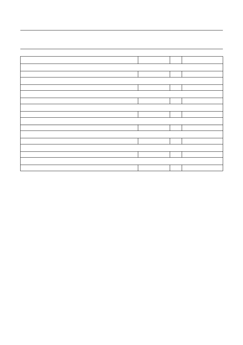
H
ORIZONTAL DELAY OF END OF VERTICAL SYNC
Horizontal end delay of vertical sync pulse at pin PVS
218 and 219
W
D10 to D0
H
ORIZONTAL SYNC PULSE START
Start of horizontal sync pulse at pin PHS
220 and 221
W
D10 to D0
H
ORIZONTAL SYNC PULSE END
End of horizontal sync pulse at pin PHS
222 and 223
W
D10 to D0
D
ATA QUALIFIER START
Start of border region and horizontal data qualifier at pin PDE
224 and 225
W
D10 to D0
D
ATA QUALIFIER END
End of border region and horizontal data qualifier at pin PDE
226 and 227
W
D10 to D0
H
ORIZONTAL ACTIVE REGION START
Start of horizontal active video region
228 and 229
W
D10 to D0
V
ERTICAL SYNC PULSE END
Vertical sync pulse end at pin PVS
230 and 231
W
D10 to D0
M
AXIMUM HORIZONTAL LINE LENGTH
Maximum reachable line length for length controlling
232 and 233
W
D10 to D0
NAME
SUBADDRESS
R/W
DATA
8.2
Clock management
8.2.1
C
LOCK GENERATION AND MULTIPLEXING
For normal operation the SAA6712E uses two clock
inputs; pin VCLK and pin CLK. VCLK is used as the
sample clock provided by the external ADCs or decoder.
The frequency and the sample edges of this clock depend
on the number of ADCs connected, or on the video dot
clock:
1 ADC mode: maximum VCLK frequency is 150 MHz
2 ADC mode: maximum VCLK frequency is 75 MHz.
The clock from pin CLK is used as an internal reference,
and it is the source clock for the internal PLL. The memory
clock MCLKO and panel clock PCLK are derived from the
PLL (see Fig.8):
N
Where N = pre-divider ratio, M = post-divider ratio and
MCLKO
CLK
16
×
=
PCLK
N
32
×
=
5 MHz
N
8 MHz
≤
≤
It is possible to drive the memory clock output directly
without the internal PLL via pin MCLKI. To achieve this the
programming flag pll_mclk must be set to logic 0.
The same is possible for the panel output clock. Therefore
the system clock CLK is used directly. The system clock is
controlled by pll_pclk which must be set to logic 0.
相關(guān)PDF資料 |
PDF描述 |
|---|---|
| SAA6713AH | XGA analog input flat panel controller |
| SAA6713H | XGA dual input flat panel controller |
| SAA7110 | Digital Multistandard Colour Decoder(數(shù)字多標(biāo)準(zhǔn)彩色譯碼器) |
| SAA7111 | Video Input Processor VIP |
| SAA7120H | Digital video encoder |
相關(guān)代理商/技術(shù)參數(shù) |
參數(shù)描述 |
|---|---|
| SAA6713AH | 制造商:PHILIPS 制造商全稱(chēng):NXP Semiconductors 功能描述:XGA analog input flat panel controller |
| SAA6713AH/V1 | 制造商:PHILIPS 制造商全稱(chēng):NXP Semiconductors 功能描述:XGA analog input flat panel controller |
| SAA6713H | 制造商:PHILIPS 制造商全稱(chēng):NXP Semiconductors 功能描述:XGA dual input flat panel controller |
| SAA6713H/V1 | 制造商:PHILIPS 制造商全稱(chēng):NXP Semiconductors 功能描述:XGA dual input flat panel controller |
| SAA6721 | 制造商:PHILIPS 制造商全稱(chēng):NXP Semiconductors 功能描述:SXGA RGB to TFT graphics engine |
發(fā)布緊急采購(gòu),3分鐘左右您將得到回復(fù)。