- 您現(xiàn)在的位置:買賣IC網(wǎng) > PDF目錄98011 > S568013MFA00E (FREESCALE SEMICONDUCTOR INC) 0-BIT, 8 MHz, OTHER DSP, PQFP32 PDF資料下載
參數(shù)資料
| 型號: | S568013MFA00E |
| 廠商: | FREESCALE SEMICONDUCTOR INC |
| 元件分類: | 數(shù)字信號處理 |
| 英文描述: | 0-BIT, 8 MHz, OTHER DSP, PQFP32 |
| 封裝: | ROHS COMPLIANT, LQFP-32 |
| 文件頁數(shù): | 19/125頁 |
| 文件大?。?/td> | 1702K |
| 代理商: | S568013MFA00E |
第1頁第2頁第3頁第4頁第5頁第6頁第7頁第8頁第9頁第10頁第11頁第12頁第13頁第14頁第15頁第16頁第17頁第18頁當(dāng)前第19頁第20頁第21頁第22頁第23頁第24頁第25頁第26頁第27頁第28頁第29頁第30頁第31頁第32頁第33頁第34頁第35頁第36頁第37頁第38頁第39頁第40頁第41頁第42頁第43頁第44頁第45頁第46頁第47頁第48頁第49頁第50頁第51頁第52頁第53頁第54頁第55頁第56頁第57頁第58頁第59頁第60頁第61頁第62頁第63頁第64頁第65頁第66頁第67頁第68頁第69頁第70頁第71頁第72頁第73頁第74頁第75頁第76頁第77頁第78頁第79頁第80頁第81頁第82頁第83頁第84頁第85頁第86頁第87頁第88頁第89頁第90頁第91頁第92頁第93頁第94頁第95頁第96頁第97頁第98頁第99頁第100頁第101頁第102頁第103頁第104頁第105頁第106頁第107頁第108頁第109頁第110頁第111頁第112頁第113頁第114頁第115頁第116頁第117頁第118頁第119頁第120頁第121頁第122頁第123頁第124頁第125頁
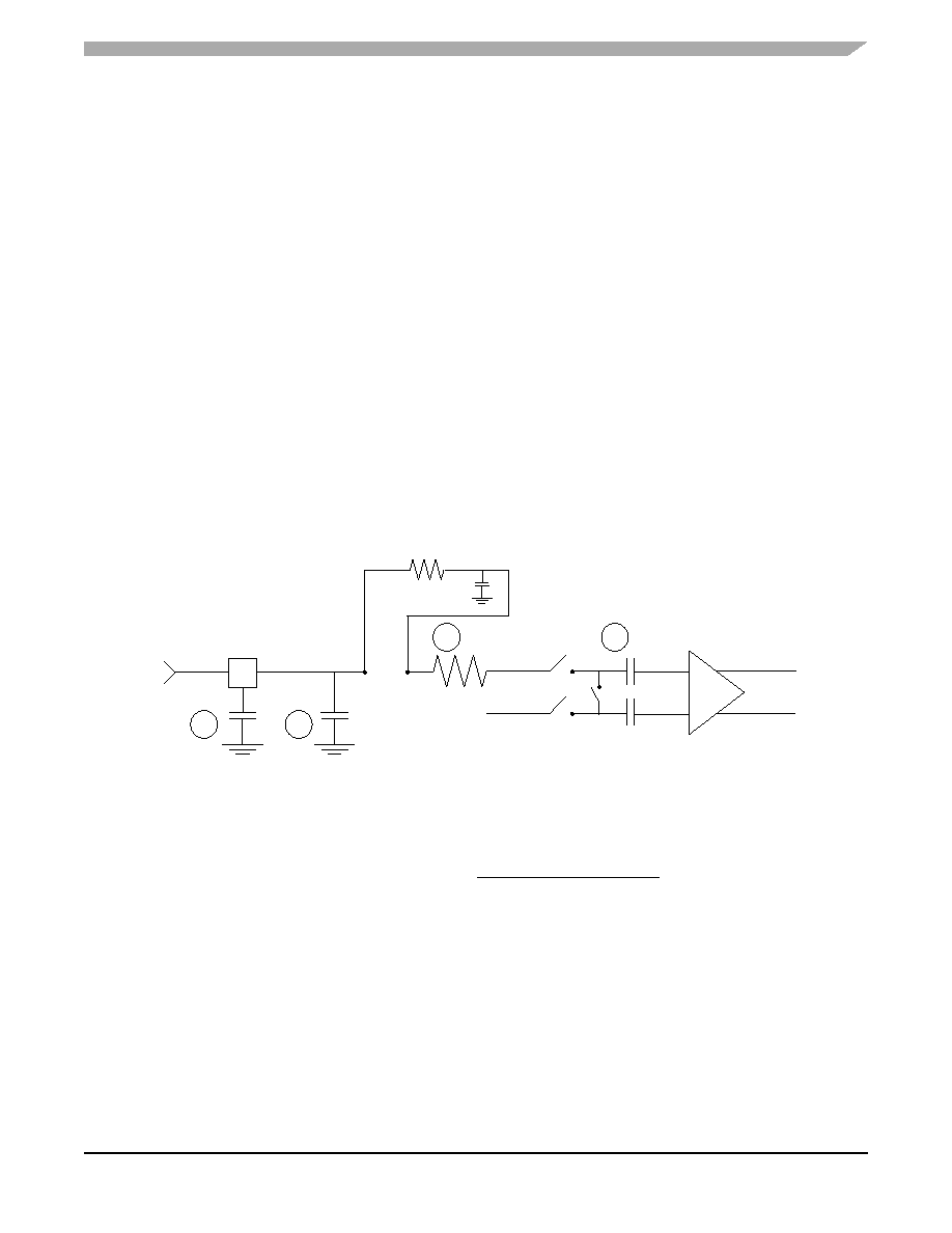
Equivalent Circuit for ADC Inputs
56F8013/56F8011 Data Sheet, Rev. 11
Freescale Semiconductor
115
10.15 Equivalent Circuit for ADC Inputs
Figure 10-17 illustrates the ADC input circuit during sample and hold. S1 and S2 are always open/closed
at the same time that S3 is closed/open. When S1/S2 are closed & S3 is open, one input of the sample and
hold circuit moves to (VREFH-VREFL)/2, while the other charges to the analog input voltage. When the
switches are flipped, the charge on C1 and C2 are averaged via S3, with the result that a single-ended
analog input is switched to a differential voltage centered about (VREFH-VREFL)/2. The switches switch
on every cycle of the ADC clock (open one-half ADC clock, closed one-half ADC clock). Note that there
are additional capacitances associated with the analog input pad, routing, etc., but these do not filter into
the S/H output voltage, as S1 provides isolation during the charge-sharing phase.
One aspect of this circuit is that there is an on-going input current, which is a function of the analog input
voltage, VREF and the ADC clock frequency.
1.
Parasitic capacitance due to package, pin-to-pin and pin-to-package base coupling; 1.8pF
2.
Parasitic capacitance due to the chip bond pad, ESD protection devices and signal routing; 2.04pF
3.
Equivalent resistance for the channel select mux; 100 ohms
4.
Sampling capacitor at the sample and hold circuit. Capacitor C1 is normally disconnected from the input and is only
connected to it at sampling time; 1.4pF
5.
Equivalent input impedance, when the the input is selected =
Figure 10-17 Equivalent Circuit for A/D Loading
10.16 Power Consumption
See Section 10.1 for a list of IDD requirements for the 56F8013/56F8011. This section provides additional
detail which can be used to optimize power consumption for a given application.
5. LSB = Least Significant Bit = 0.806mV
6. Pin groups are detailed following Table 10-1.
7. For device S56F8013MFA00E, input leakage current is ± 1
μA.
8. The current that can be injected or sourced from an unselected ADC signal input without impacting the performance of the
ADC.
1
2
3
Analog Input
4
S1
S2
S3
C1
C2
S/H
C1 = C2 = 1pF
(VREFH- VREFL )/ 2
125
Ω ESD Resistor
8pF noise damping capacitor
1
(ADC Clock Rate) x 1.4 x 10⁻¹²
相關(guān)PDF資料 |
PDF描述 |
|---|---|
| MC56F8023VLC | 16-BIT, FLASH, 32 MHz, MICROCONTROLLER, PQFP32 |
| MC56F8033VLC | 16-BIT, FLASH, 32 MHz, MICROCONTROLLER, PQFP32 |
| MC56F8347MPY60 | 16-BIT, 120 MHz, OTHER DSP, PQFP160 |
| MC56F8355VFG60 | 4-BIT, 120 MHz, OTHER DSP, PQFP128 |
| MC56F8355MFG60 | 4-BIT, 120 MHz, OTHER DSP, PQFP128 |
相關(guān)代理商/技術(shù)參數(shù) |
參數(shù)描述 |
|---|---|
| S5-680RF1 | 制造商:Riedon 功能描述:RES 680 OHM 4W 1% WW SMD |
| S5688B | 制造商:TOSHIBA 制造商全稱:Toshiba Semiconductor 功能描述:TOSHIBA Rectifier Silicon Diffused Type |
| S5688B(Q) | 制造商:Toshiba 功能描述:Diode 100V 1A 2-Pin DO-41SS |
| S5688B(TPA2) | 制造商:Toshiba America Electronic Components 功能描述:Diode 100V 1A 2-Pin DO-41SS T/R Cut Tape |
| S5688G | 制造商:Toshiba America Electronic Components 功能描述: 制造商:Panasonic Industrial Company 功能描述:DIODE |
發(fā)布緊急采購,3分鐘左右您將得到回復(fù)。