- 您現(xiàn)在的位置:買(mǎi)賣(mài)IC網(wǎng) > PDF目錄383645 > MT90812 (Mitel Networks Corporation) Integrated Digital Switch (IDX)(集成數(shù)字開(kāi)關(guān)) PDF資料下載
參數(shù)資料
| 型號(hào): | MT90812 |
| 廠(chǎng)商: | Mitel Networks Corporation |
| 英文描述: | Integrated Digital Switch (IDX)(集成數(shù)字開(kāi)關(guān)) |
| 中文描述: | 綜合數(shù)字交換機(jī)(IDX的)(集成數(shù)字開(kāi)關(guān)) |
| 文件頁(yè)數(shù): | 5/105頁(yè) |
| 文件大?。?/td> | 334K |
| 代理商: | MT90812 |
第1頁(yè)第2頁(yè)第3頁(yè)第4頁(yè)當(dāng)前第5頁(yè)第6頁(yè)第7頁(yè)第8頁(yè)第9頁(yè)第10頁(yè)第11頁(yè)第12頁(yè)第13頁(yè)第14頁(yè)第15頁(yè)第16頁(yè)第17頁(yè)第18頁(yè)第19頁(yè)第20頁(yè)第21頁(yè)第22頁(yè)第23頁(yè)第24頁(yè)第25頁(yè)第26頁(yè)第27頁(yè)第28頁(yè)第29頁(yè)第30頁(yè)第31頁(yè)第32頁(yè)第33頁(yè)第34頁(yè)第35頁(yè)第36頁(yè)第37頁(yè)第38頁(yè)第39頁(yè)第40頁(yè)第41頁(yè)第42頁(yè)第43頁(yè)第44頁(yè)第45頁(yè)第46頁(yè)第47頁(yè)第48頁(yè)第49頁(yè)第50頁(yè)第51頁(yè)第52頁(yè)第53頁(yè)第54頁(yè)第55頁(yè)第56頁(yè)第57頁(yè)第58頁(yè)第59頁(yè)第60頁(yè)第61頁(yè)第62頁(yè)第63頁(yè)第64頁(yè)第65頁(yè)第66頁(yè)第67頁(yè)第68頁(yè)第69頁(yè)第70頁(yè)第71頁(yè)第72頁(yè)第73頁(yè)第74頁(yè)第75頁(yè)第76頁(yè)第77頁(yè)第78頁(yè)第79頁(yè)第80頁(yè)第81頁(yè)第82頁(yè)第83頁(yè)第84頁(yè)第85頁(yè)第86頁(yè)第87頁(yè)第88頁(yè)第89頁(yè)第90頁(yè)第91頁(yè)第92頁(yè)第93頁(yè)第94頁(yè)第95頁(yè)第96頁(yè)第97頁(yè)第98頁(yè)第99頁(yè)第100頁(yè)第101頁(yè)第102頁(yè)第103頁(yè)第104頁(yè)第105頁(yè)
Advance Information
MT90812
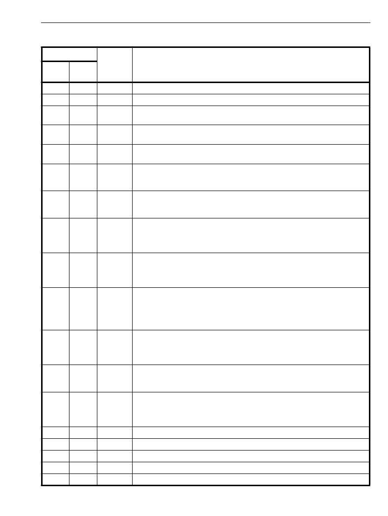
5
33-34
59-61
NC
No Connect
. Ground
35
62
VSS2
Ground
.
36-37
63-64
STi0-1
Serial TDM input streams 0 and 1 (Input)
. Serial data input streams which have
data rates of 2.048 Mb/s with 32 channels.
38-39
65-66
STo0-1
Serial TDM output streams 0 and 1 (Three-state output)
. Serial data output
streams which have data rates of 2.048 Mb/s with 32 channels.
40
67
DPER
D-Channel Input in ST-BUS format (Input)
. The MT8952B CDSTo stream
containing formatted D-channel data.
41
68
EST0
Expansion Bus Serial data stream 0 (Three-state output/input)
. This is a bi-
directional pin at 8.192 Mb/s in IDX Link mode. In TDM Link mode this is a 2.048,
4.096 or 8.192 Mb/s output stream.
42
1
EST1
Expansion Bus Serial data stream 1 (Three-state output/input)
. This is a bi-
directional pin at 8.192 Mb/s in IDX Link mode. In TDM Link mode this is a 2.048,
4.096 or 8.192 Mb/s input stream.
43
2
ODE
Output Device Enable (Input)
. This is the output enable input for the serial
outputs. If this input is low, STo0, STo1, EST0, EST1 are high impedance. If this
input is high, each channel may still be put into high impedance state by using per
channel control bit in the Connection Memory.
44
3
C8
Clock 8.192 (Bidirectional)
. As an input this signal is used for Expansion bus
and/or internal clock source at 8.192 MHz depending on the timing mode
selected. As an output this signal is an 8.192 MHz output clock locked to the
reference input signal.
45
4
F8
Frame Pulse for 8.192 MHz (Bidirectional)
. As an input accepts and
automatically identifies frame synchronization signals formatted according to ST-
BUS and GCI interface specifications. As an output is an 8 KHz frame pulse that
indicates the start of the active frame. Either F8 or FPi are used for frame
synchronization depending on the timing mode selected
46
5
C8P_C16i
Oscillator Master Clock (CMOS Input)
. For crystal operation, a 8.192MHz
crystal is connected to this pin from OSCo. For clock oscillator operation, this pin
is connected to a clock source. The clock source of either 8.192 MHz or 16.384
MHz can be used as selected in the Timing Control Register (TC).
47
6
OSCo
Oscillator Master Clock (CMOS Output)
. For crystal operation, a 8.192MHz
crystal is connected from this pin to C8P_C16i. For clock oscillator operation, this
pin is left unconnected.
48
7
FPi
Frame Pulse (Input).
This input accepts and automatically identifies frame
synchronization signals formatted according to ST-BUS and GCI interface
specifications. Either F8 or FPi are used for frame synchronization depending on
the timing mode selected.
49
8
C4i
Clock 4.096 MHz (Input)
. This input is the 4.096 MHz clock input.
-
9
NC
No Connect
. Ground
50-51
10-11
IC
Internal Connect
. Open.
52
12
VSSA
Analog Ground
.
53
13
VDDA
+5 Volt Power Supply (Analog)
.
Pin Description (continued)
Pin #
Name
Description
64 Pin
MQFP
68 Pin
PLCC
相關(guān)PDF資料 |
PDF描述 |
|---|---|
| MT90840AK | Distributed Hyperchannel Switch |
| MT90840AP | Distributed Hyperchannel Switch |
| MT9085B | PAC - Parallel Access Circuit(并行存取電路) |
| MT9092 | Digital Telephone with HDLC(數(shù)字電話(huà)(帶高階數(shù)據(jù)鏈路控制HDLC)) |
| MT9092 | ISO2-CMOS ST-BUS⑩ FAMILY Digital Telephone with HDLC (HPhone-II) |
相關(guān)代理商/技術(shù)參數(shù) |
參數(shù)描述 |
|---|---|
| MT90812AL | 制造商:Microsemi Corporation 功能描述:SWIT FABRIC 192 X 192 16.384MBPS 5V 64MQFP - Trays 制造商:Zarlink Semiconductor Inc 功能描述:SWIT FABRIC 192 X 192 16.384MBPS 5V 64MQFP - Trays |
| MT90812AL1 | 制造商:Microsemi Corporation 功能描述:SWIT FABRIC 192 X 192 16.384MBPS 5V 64MQFP - Trays 制造商:Microsemi Corporation 功能描述:PB FREE INTEGRATED DIGITAL SWITCH |
| MT90812AP | 制造商:MITEL 制造商全稱(chēng):Mitel Networks Corporation 功能描述:Integrated Digital Switch (IDX) |
| MT90812AP1 | 制造商:Zarlink Semiconductor Inc 功能描述:SWIT FABRIC 192 X 192 16.384MBPS 5V 68PLCC /BAKE/DRYPACK - Rail/Tube 制造商:Zarlink Semiconductor Inc 功能描述:INTEGRATED DIGITAL SWCH |
| MT90812APR | 制造商:Microsemi Corporation 功能描述:SWIT FABRIC 192 X 192/64 X 64 1.048GBPS 5V 68PLCC - Tape and Reel |
發(fā)布緊急采購(gòu),3分鐘左右您將得到回復(fù)。