- 您現(xiàn)在的位置:買賣IC網(wǎng) > PDF目錄383645 > MT90812 (Mitel Networks Corporation) Integrated Digital Switch (IDX)(集成數(shù)字開(kāi)關(guān)) PDF資料下載
參數(shù)資料
| 型號(hào): | MT90812 |
| 廠商: | Mitel Networks Corporation |
| 英文描述: | Integrated Digital Switch (IDX)(集成數(shù)字開(kāi)關(guān)) |
| 中文描述: | 綜合數(shù)字交換機(jī)(IDX的)(集成數(shù)字開(kāi)關(guān)) |
| 文件頁(yè)數(shù): | 4/105頁(yè) |
| 文件大小: | 334K |
| 代理商: | MT90812 |
第1頁(yè)第2頁(yè)第3頁(yè)當(dāng)前第4頁(yè)第5頁(yè)第6頁(yè)第7頁(yè)第8頁(yè)第9頁(yè)第10頁(yè)第11頁(yè)第12頁(yè)第13頁(yè)第14頁(yè)第15頁(yè)第16頁(yè)第17頁(yè)第18頁(yè)第19頁(yè)第20頁(yè)第21頁(yè)第22頁(yè)第23頁(yè)第24頁(yè)第25頁(yè)第26頁(yè)第27頁(yè)第28頁(yè)第29頁(yè)第30頁(yè)第31頁(yè)第32頁(yè)第33頁(yè)第34頁(yè)第35頁(yè)第36頁(yè)第37頁(yè)第38頁(yè)第39頁(yè)第40頁(yè)第41頁(yè)第42頁(yè)第43頁(yè)第44頁(yè)第45頁(yè)第46頁(yè)第47頁(yè)第48頁(yè)第49頁(yè)第50頁(yè)第51頁(yè)第52頁(yè)第53頁(yè)第54頁(yè)第55頁(yè)第56頁(yè)第57頁(yè)第58頁(yè)第59頁(yè)第60頁(yè)第61頁(yè)第62頁(yè)第63頁(yè)第64頁(yè)第65頁(yè)第66頁(yè)第67頁(yè)第68頁(yè)第69頁(yè)第70頁(yè)第71頁(yè)第72頁(yè)第73頁(yè)第74頁(yè)第75頁(yè)第76頁(yè)第77頁(yè)第78頁(yè)第79頁(yè)第80頁(yè)第81頁(yè)第82頁(yè)第83頁(yè)第84頁(yè)第85頁(yè)第86頁(yè)第87頁(yè)第88頁(yè)第89頁(yè)第90頁(yè)第91頁(yè)第92頁(yè)第93頁(yè)第94頁(yè)第95頁(yè)第96頁(yè)第97頁(yè)第98頁(yè)第99頁(yè)第100頁(yè)第101頁(yè)第102頁(yè)第103頁(yè)第104頁(yè)第105頁(yè)
MT90812
Advance Information
4
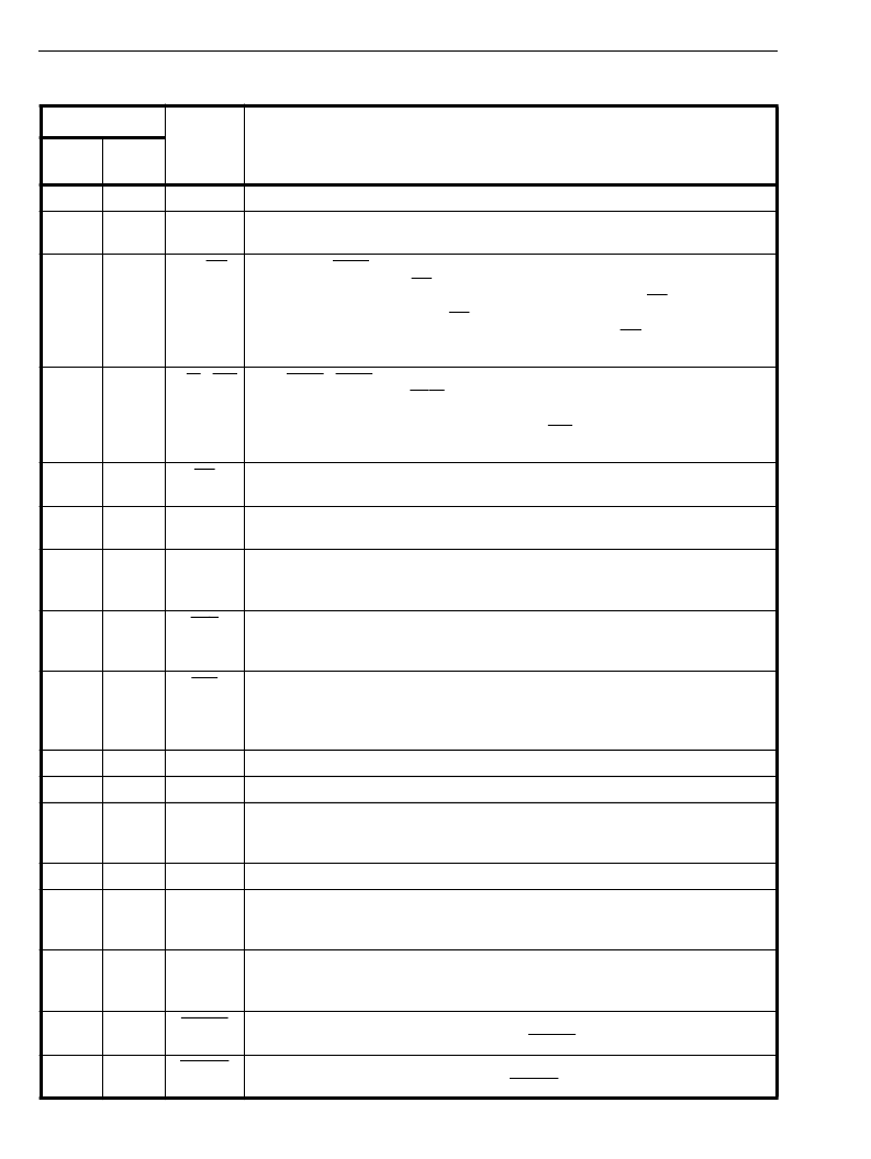
Pin Description
Pin #
Name
Description
64 Pin
MQFP
68 Pin
PLCC
1
25-26
NC
No Connect
. Ground
2-11
27-36
A0 - A9
Address 0 - 9(Input)
. When non-multiplexed CPU bus is selected, these lines
provide the A0 - A9 address lines to IDX internal memories.
12
37
DS/RD
Data Strobe/Read (Input)
. For Motorola multiplexed bus operation, this active
high DS input works with CS to enable the read and write operations.
For Motorola non-multiplexed CPU bus operation, this input is DS. This active low
input works in conjunction with CS to enable the read and write operations.
For Intel/National multiplexed bus operations, this input is RD. This active low
input sets the data bus lines (AD0-AD7) as outputs.
13
38
R/W \ WR
Read/Write \ Write (Input)
. In case of non-multiplexed and Motorola multiplexed
buses, this input is Read/Write. This input controls the direction of the data bus
lines (AD0 - AD7) during a microprocessor access.
For Intel/National multiplexed bus, this input is WR. This active low signal
configures the data bus lines (AD0-AD7) as inputs.
14
39
CS
Chip Select (Input)
. Active low input enabling a microprocessor read or write of
internal memories.
15
40
AS/ALE
Address Strobe or Latch Enable (Input)
. This input is only used if multiplexed
bus is selected via IM input pin.
16
41
IM
CPU Interface Mode (Input)
. If High, this input sets the device in the multiplexed
microprocessor mode. If this input is grounded, the device resumes non-
multiplexed CPU interface.
17
42
DTA
Data Acknowledgment (Open Drain Output)
. This active low output indicates
that a data bus transfer is complete. A 10Kohm pull-up resistor is required at this
output.
18
43
IRQ
Interrupt Request Output (Open Drain Output)
. This active low output notifies
the controlling microprocessor of an interrupt request. It goes Low only when the
bits in the Interrupt Enable Register are programmed to acknowledge the source
of the interrupt as defined in the Interrupt Status Register.
-
44
NC
No Connect
. Ground
19
45
VSS5
Ground
.
20-27
46-53
AD0 - AD7
Data Bus (Bidirectional)
. These pins provide microprocessor access to the
internal memories. In the multiplexed bus mode, these pins also provide the input
address to the internal Address Latch circuit.
28
54
VSS1
Ground
.
29
55
TEOP
Transmit End of Packet (Input)
. This is a strobe that is generated by the HDLC
controller chip for one bit period during the last bit of the closing flag of the
transmit packet.
30
56
REOP
Receive End of Packet (Input)
. A receive packet will normally be terminated
when the HDLC controller asserts the REOP strobe for one bit period, one bit time
after the closing flag is received.
31
57
TxCEN
Transmit Clock Enable (Output)
. The HDLC transmitter is controlled by the IDX-
generated Transmit Clock Enable signal, TxCEN.
32
58
RxCEN
Receive Clock Enable (Output)
. The HDLC receiver is controlled by the IDX-
generated Receive Clock Enable signal, RxCEN.
相關(guān)PDF資料 |
PDF描述 |
|---|---|
| MT90840AK | Distributed Hyperchannel Switch |
| MT90840AP | Distributed Hyperchannel Switch |
| MT9085B | PAC - Parallel Access Circuit(并行存取電路) |
| MT9092 | Digital Telephone with HDLC(數(shù)字電話(帶高階數(shù)據(jù)鏈路控制HDLC)) |
| MT9092 | ISO2-CMOS ST-BUS⑩ FAMILY Digital Telephone with HDLC (HPhone-II) |
相關(guān)代理商/技術(shù)參數(shù) |
參數(shù)描述 |
|---|---|
| MT90812AL | 制造商:Microsemi Corporation 功能描述:SWIT FABRIC 192 X 192 16.384MBPS 5V 64MQFP - Trays 制造商:Zarlink Semiconductor Inc 功能描述:SWIT FABRIC 192 X 192 16.384MBPS 5V 64MQFP - Trays |
| MT90812AL1 | 制造商:Microsemi Corporation 功能描述:SWIT FABRIC 192 X 192 16.384MBPS 5V 64MQFP - Trays 制造商:Microsemi Corporation 功能描述:PB FREE INTEGRATED DIGITAL SWITCH |
| MT90812AP | 制造商:MITEL 制造商全稱:Mitel Networks Corporation 功能描述:Integrated Digital Switch (IDX) |
| MT90812AP1 | 制造商:Zarlink Semiconductor Inc 功能描述:SWIT FABRIC 192 X 192 16.384MBPS 5V 68PLCC /BAKE/DRYPACK - Rail/Tube 制造商:Zarlink Semiconductor Inc 功能描述:INTEGRATED DIGITAL SWCH |
| MT90812APR | 制造商:Microsemi Corporation 功能描述:SWIT FABRIC 192 X 192/64 X 64 1.048GBPS 5V 68PLCC - Tape and Reel |
發(fā)布緊急采購(gòu),3分鐘左右您將得到回復(fù)。